High resolution PWM requirements for WBG power converters
The need for high PWM resolution
Modern power electronics make extensive use of digital control systems. Compared with their analog counterparts, these offer unprecedented flexibility and computational power. However, a fundamental bottleneck exists at the interface between the discrete-time digital world and the continuous-time analog one: quantization. While digital control now frequently operates with 32-bit precision, the actual precision of the control output remains limited by the physical temporal resolution of the PWM generator, which can be significantly lower.
With wide-bandgap (WBG) semiconductors, the short switching period drastically reduces the relative PWM resolution. For instance, at 1 MHz, the PWM resolution of a modulator running on a 100 MHz base clock is inevitably less than 7 bits. This introduces non-linearities that can result in excessive harmonic distortion or steady-state instabilities. In this context, High-Resolution Pulse-Width Modulation (HR-PWM) has emerged as a critical requirement for mitigating quantization-induced non-linearities and enabling the stable operation of medium-frequency converters.
This article explains why high-resolution pulse-width modulation (PWM) is nowadays becoming a de facto requirement for digital control systems. It also shows how the corresponding challenges are addressed inside imperix’s latest controller: the B-Box 4.
High-resolution demands in DAB converters
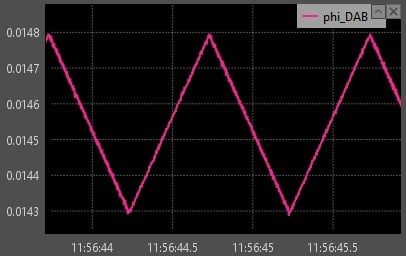
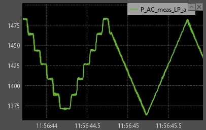
An illustration of quantization-related limitations is provided by DAB converters, which are widespread in electric vehicle charging stations, solid-state transformers, and energy storage systems. Using the conventional Single Phase Shift (SPS) modulation scheme, the power transfer is controlled exclusively by the phase shift (between the primary and the secondary) according to:
To maximize power density, design engineers tend to increase the switching frequency aggressively. At the same time, although the leakage inductance is minimized, other parameters from the above equation remain high. As a result, the power transfer is highly sensitive to the phase shift, because an extremely small timing increment can already cause a substantial shift in power.
For instance, in a 10kW/100kHz DAB, a single discrete step of 10 ns can instantly result in a step of several hundred watts. Such coarse granularity renders precise control of the output current or voltage very challenging. The closed-loop controller may suffer from limit cycling and steady-state tracking errors, and may even inject significant low-frequency current ripples into the battery.
Quantization-induced non-linearities
For closed-loop control, two quantization processes occur: first within the analog-to-digital converter (ADC) and second within the pulse-width modulator (PWM). These two processes represent the main sources of non-linearities, followed by stochastic timing uncertainties (jitter) with significantly less impact.
These phenomena not only result in a proportionally less accurate output but also trigger a cascade of non-linear control effects, steady-state inaccuracies, and hardware-level distortions. Eventually, these effects limit the maximum achievable closed-loop bandwidth and may even introduce undesirable steady-state behaviors, such as limit-cycle oscillations (LCOs).
Amplitude quantization in ADC inputs
Fundamentally, an ADC performs two distinct operations: sampling and quantization. Sampling converts a continuous-time analog signal into a discrete-time sequence of measurement points, while quantization maps the continuous voltage levels into a finite set of digital codes. The smallest measurable change of amplitude that results in different digital codes is known as resolution. This is commonly expressed as an absolute quantity (e.g., a number of millivolts) or as a fraction of the full-scale range (e.g., a number of bits).
The quantization error is the difference between the actual analog value and its quantized representation. Assuming that the signal is of significant amplitude and uncorrelated to the sampling clock, the quantization error is white noise such that:
with representing the ADC resolution.
Temporal quantization in PWM outputs
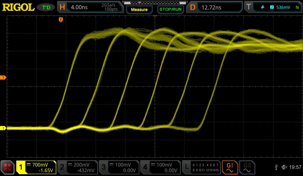
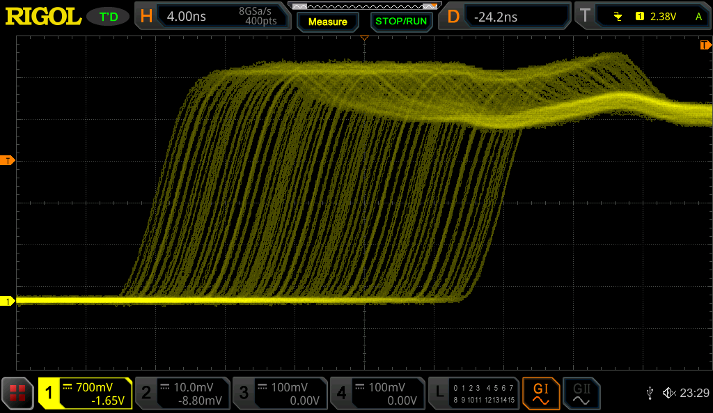
Digital pulse-width modulators also operate with quantization-related performance boundaries. In fact, unlike their analog counterparts, a digital modulator can adjust the PWM signal edges only in discrete increments due to the presence of clocked digital logic. Eventually, the temporal resolution of a modulator is inevitably dictated by the frequency of its base clock.
The table below shows that the resolution offered by conventional PWM resources drops drastically when a high switching frequency is selected.
| Switching freq. | Clock frequency | Time resolution | Resolution |
| 100kHz | 100MHz | 10ns | 10bits |
| 3MHz | 100MHz | 10ns | 5bits |
| 1MHz | 1GHz | 1ns | 10bits |
| 1MHz | 4GHz | 250ps | 12bits |
| 100kHz | 4GHz | 250ps | >15bits |
Consequences of low PWM resolution
Limit Cycle Oscillations (LCOs)
The most common and visible consequence of limited PWM and ADC resolution is the emergence of Limit Cycle Oscillations (LCOs). LCOs are sustained periodic steady-state oscillations that occur at frequencies below the switching frequency. Such oscillations are highly undesirable because their exact amplitude and frequency are notoriously difficult to predict.
LCOs arise from the control system continuously toggling between two quantization levels, corresponding to small negative and small positive errors. In fact, as the system cannot produce (PWM limitation) or measure (ADC limitation) the exact quantities that correspond to a zero error, toggling between the two nearest states is inevitable, resulting in a low-frequency oscillation on the output.
To eliminate LCOs, the PWM’s resolution must be finer than the ADC’s [1], i.e.:
However, even if this condition is met, LCOs can still occur due to inadequate controller design or tuning. For instance, without an integral term, the controller inevitably relies on a nonzero error to drive the output. Additionally, a high proportional gain (Kp) can also cause the duty cycle to jump over multiple ADC values in response to a single-bit error. Eliminating LCOs, therefore, requires rigorously adhering to non-trivial mathematical conditions. These are summarized below and further described in [1]:
| Design criteria | Condition | Justification |
| PWM resolution | At least one PWM value should map into the zero-error ADC value. | |
| Integral gain | Some integral action is required, but without an oscillatory behavior. | |
| Loop gain | The non-linear gain of the quantizer should not lead to oscillations. |
Impact on dead time compensation
In power electronics, inserting a dead-time between complementary switching commands is essential to prevent destructive shoot-through currents. On the other hand, it is also a known and important source of non-linearity.
Low PWM resolution rarely forces a higher dead-time than strictly necessary. However, it may nonetheless force a coarse dead time selection. Consequently, because dead-time compensation requires extremely fine adjustments to the pulse width, perfect compensation is practically impossible without sufficient PWM resolution.
Elevated noise floor
PWM-related quantization noise manifests as a broadband noise injected straight into the controlled variable(s). Unlike dead-time distortion that concentrates its energy at predictable multiples of the fundamental (e.g., the 5th and 7th harmonics), quantization noise uniformly elevates the entire spectral noise floor. In systems with an exceptionally low noise floor, PWM-related quantization noise may hence become the dominant noise source.
Torque ripple and mechanical resonances
In precision motor drives, low PWM resolution prevents the synthesis of smooth sine waves, resulting in “stair-stepped” current trajectories. These inaccuracies create torque ripple, which eventually manifests as vibration and acoustic noise. If these ripple frequencies align with the system’s mechanical resonance, they may even accelerate component wear and fatigue.
EMI spectral peaking
To some extent, low PWM resolution also hinders the use of advanced electromagnetic interference (EMI) mitigation techniques such as spread spectrum. These strategies require fine-tuned frequency dithering to flatten the EMI spectrum. However, low PWM resolution forces coarse frequency steps, which reduces the spreading effect.
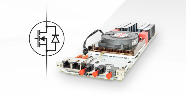
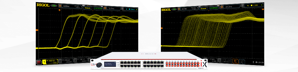
High resolution PWM at Imperix
At imperix, high-resolution modulation (HR-PWM) is exclusively supported by the B-Box 4, which features a hardware-based implementation with a resolution of 250 ps.
Third-party configuration
(12-bit ADC / 10-bit PWM)
This corresponds to the typical performance of standard microcontrollers.
- Steady-state instability: The 10-bit PWM offers only 1024 steps while the 12-bit ADC offers 4096 levels. There is thus a high probability that no duty cycle perfectly corresponds to the zero-error ADC value. Consequently, the system perpetually toggles between the two nearest PWM steps, creating a self-sustained LCO.
- Bandwidth constraints: To avoid LCOs, the control engineer must reduce the loop gain and/or implement aggressive low-pass filtering. This typically limits the achievable closed-loop frequency to avoid instability.
Imperix B-Box 4
(16-bit ADC / 18-bit PWM)
This corresponds to the performance achievable by the B-Box 4.
- Analog-like performance: With 16 bits of native resolution – or over 20 bits of effective resolution with synchronous averaging (below 1Msps), ADC quantization noise is below other sources (e.g., sensors) and its effect is hence negligible.
- HR-PWM implementation: With over 17 bits of PWM resolution, the first condition for LCO-free operation is met for switching frequencies below 32kHz. Furthermore, with over 10 bits up to 1 MHz, PWM-related quantization noise remains comparable to that of most sensors.
Mitigation strategies
High-resolution pulse-width modulation (HR-PWM)
Specialized microcontrollers incorporate dedicated silicon-level (ASIC) resources to achieve sub-nanosecond edge placement. For instance, the TI C2000 series uses a proprietary block known as the Micro-Edge Positioner (MEP). This yields a typical resolution of as little as 150 ps.
In FPGAs, achieving similar PWM resolution is physically impossible with standard counter-based architectures (because the system clock would need to be in the multi-GHz range). Consequently, engineers rely on different approaches, leveraging specialized hardware resources to circumvent the clock frequency barrier:
- Phase-shifted clocks: A digital clock manager or Phase-Locked Loop (PLL) generates multiple phase-shifted clocks (e.g., 0°, 90°, 180°, 270°). Subsequently, a multiplexer selects the specific phase edge to trigger the final output flip-flop.
- Serializer/deserializer resources: Special primitives (such as OSERDES in the AMD/Xilinx family) are used to perform parallel-to-serial conversion. With that approach, a low-speed parallel word containing the fractional-duty-cycle data can be clocked out serially at high transmission rates (multi-GHz).
- Tapped delay chains: A reference pulse propagates through an unclocked analog delay line comprising cascaded logic gates, buffers, or dedicated delay primitives (e.g., Xilinx/AMD’s IDELAY2). A multiplexer subsequently selects the appropriate physical tap to output the signal based on the LSBs of the duty cycle command.
Dithering approaches
For very high switching frequencies (typically above 5MHz), the physically achievable resolution of the modulator is inevitably low. In this case, signal processing is typically employed to deliberately toggle the duty cycle between two adjacent quantization levels, thereby controlling the average output over some time interval. Different algorithms can be used to decide when to switch between the adjacent duty cycles:
- Fractional dithering: A repetitive sequence is used, for instance, implementing a 3x/1x alternating pattern to generate a 25% intermediary level. While simple to implement, regular patterns inject undesirable sub-harmonics into the system.
- White noise dithering: A random sequence is generated to spread the error energy evenly across the frequency spectrum, reducing noticeable sub-harmonics while also raising the overall noise floor.
- Sigma-delta noise shaping: The high-resolution, low-frequency control output is evaluated by a low-resolution, high-speed quantizer that is part of a negative feedback loop. By accumulating the quantization error, the feedback loop acts as a high-pass filter pushing quantization noise into higher frequencies, where the converter’s low-pass output filter provides sufficient attenuation [2].
Conclusion
In real-world conditions, the performance of a closed-loop digital control system is determined not only by the processing system and the implemented control algorithm. Ultimately, it is also constrained by finite resolution and timing uncertainty. The limited temporal resolution of the modulator notably introduces discrete voltage steps that, if coarser than the ADC’s resolution, may lead to limit-cycle oscillations unless adequate control design and/or filtering is implemented.
While older silicon-based systems operating at tens of kilohertz could tolerate lower resolution through heavy low-pass filtering, modern WBG converters are facing a true bottleneck due to the resolution-bandwidth conflict. Additionally, for demanding topologies such as DABs, the high mathematical sensitivity of power transfer to the phase-shift angle renders standard clock-bound resolution strictly infeasible, regardless of the control bandwidth.
Achieving high-performance control in the MHz range requires leveraging high-resolution hardware architectures or advanced modulation and signal-processing techniques to mitigate the fundamental nonlinearities of the digital domain. As switching frequencies continue to increase, advanced, ultra-linear HR-PWM architectures will move from a high-end option to an essential for achieving ultimate power density and conversion fidelity.
References
- A. Peterchev and S. Sanders, “Quantization Resolution and Limit Cycling in Digitally Controlled PWM Converters”, in IEEE Proc. of PESC Conference, Vancouver, 2001.
- M. Norris, L. M. Platon, E. Alarcon, and D. Maksomivic, “Quantization Noise Shaping in Digital PWM Converters”, in IEEE Proc. of PESC Conference, Rhodes, 2008.