Table of Contents
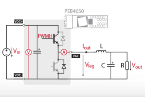
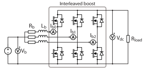
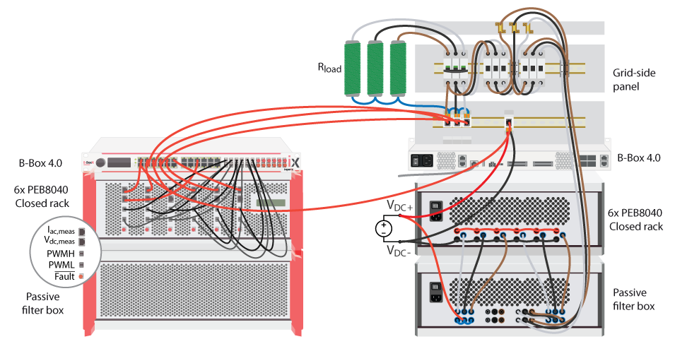
This page provides first-time users of the power electronics bundle with step-by-step guidance for implementing a simple application, which can also serve as a self-commissioning protocol. The chosen example is a simplified version of the 3-phase PV inverter for grid-tied applications. The main differences are that a three-phase resistive load is used and that the single-leg boost converter is replaced by an interleaved boost, enabling all six power modules to be used and tested. The schematic of the system is depicted in Fig. 1.
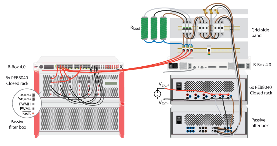
Components of the power electronics bundle
The power electronics bundle includes the following products:
- B-Box 4: It enables the experimental validation of power converter control techniques. It has 24 analog channels and 24 optical PWM outputs. More information and a detailed quick start guide can be found here and here, respectively.
- 6x PEB-800-40 power modules: They contain two SiC MOSFETs and are rated for 800V DC and 40A RMS. Detailed information and a quick start guide can be found here and here, respectively.
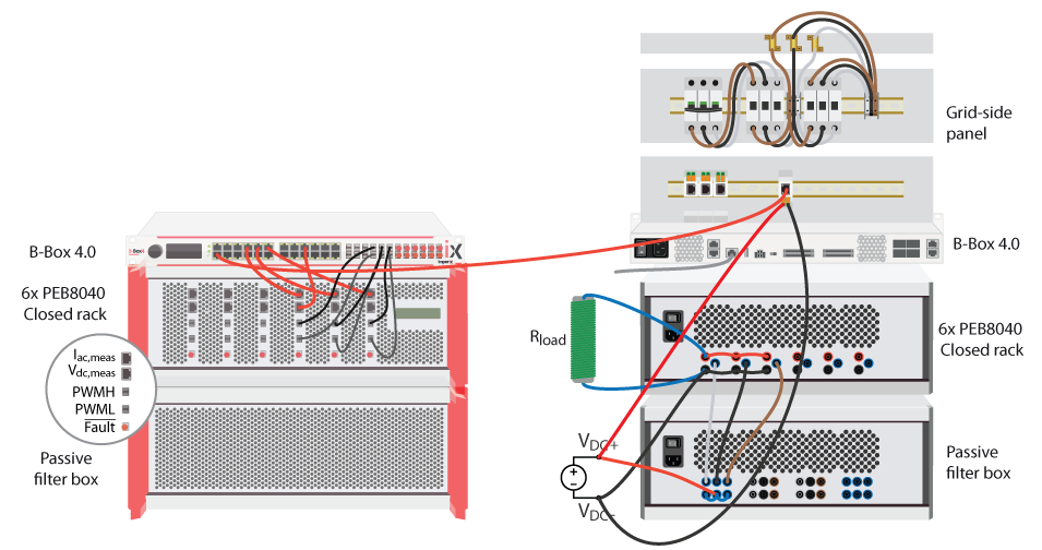
- Passive filter box: It includes six power inductors and two EMC filters with star-connected capacitors. Additionally, the standard closed rack allows these components to be connected using banana cables. More information can be found here.
- Grid side panel: It provides the necessary circuit breaker and connection relays that allow the implementation of grid-tied inverters in a safe manner. More information can be found here.
- External current and voltage sensors: Four CSR-25-HWB isolated current sensors rated for 25A, three VSR-500-HBW non-isolated voltage sensors rated for 500V and three VSR-1000-HBW isolated voltage sensors rated for 1000V are included in the power electronics bundle.
Installing the software
To program its controllers, imperix provides two Software Development Kits (SDKs):
- The ACG SDK for Automated Code Generation (ACG) from Simulink or PLECS.
- The CPP SDK for development using C/C++ code.
The following sections are dedicated to the ACG SDK, which contains plug-in blocksets for MATLAB Simulink and PLECS. It therefore requires a recent version of either software, along with the code generation tools. Detailed instructions for installing the SDK can be found in the Installation guide for imperix ACG SDK. Essentially, the main steps can be summarized as:
- Installing (if not done already) the third-party tools, namely Simulink or PLECS, along with the required code generation add-ons.
- Downloading and running the installer for the ACG SDK. Download links for either SDKs are available on https://imperix.com/downloads/.
- For Simulink, a MEX compiler for C++ must be installed. The imperix installer takes care of the rest of the configuration.
- For PLECS, the path of the freshly installed Imperix_Controllers target support package (
C:\imperix\BB3_ACG_SDK\plecsby default) must be added to the PLECS Target support packages path in the PLECS preferences.
For users of the CPP SDK, guidance regarding installation and first steps can be found in PN146.
Programming the controller
The first step consist in developing the Simulink/PLECS control model. Users can either start from an example available on the the knowledge base, or start from scratch using a template (available in the installation folder).
With the imperix ACG SDK, the same Simulink/PLECS model can serve for both offline simulation as well as code generation. More details on the first steps with the ACG SDK are given in PN134. Specific advice for running simulations in Simulink or PLECS are given in PN135 and PN137, respectively.
Once the control algorithms have been implemented (and possibly validated in simulation), equivalent code must be generated, compiled, and uploaded to the controller. With the ACG SDK, this process is automated and finishes by automatically launching Cockpit, imperix’s real-time monitoring software. From Cockpit, connecting to the target controller and uploading the run-time executable only requires a few clicks. More detailed information is given in PN138.
Equivalent steps with the C/C++ workflow are presented in PN146.
Hardware-related configuration
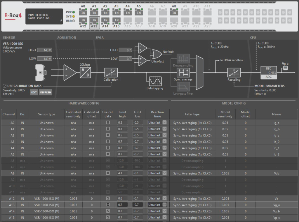
Analog inputs
An important step before running experiments consist in properly configuring the analog inputs. Indeed, proper scaling of the measurement is essential to the correct execution of the control algorithms, which is something that is not tested in simulation. Besides, the correct configuration of the Over-current and over-voltage protections is key to the equipment’s protection.
As imperix controllers possess slightly different hardware implementations (read more in PN250), the configuration of analog inputs differs as well (see table below). Nonetheless, all controllers implement two disting sets of settings:
- Software or model settings. These must be configured within the Simulink/PLECS model. This notably involves selecting the right sensor sensitivity and sampling strategy.
- Hardware settings. These primarily concern the safety limits (for protection purposes). With B-Box RCP3.0, the low-pass filters are also hardware settings.
| B-Box 4 | B-Box RCP3.0 | |
|---|---|---|
| Configuration of the software part of the analog inputs | In Simulink / PLECS / C++ code See ADC block | In Simulink / PLECS / C++ code See ADC block |
| Configuration of the hardware part of the analog inputs | Using the front panel or Cockpit See PN252 | Using the front panel See PN105 |
In this example, a B-Box 4 is used, with its analog I/Os configured as follows:
PWM outputs
The correct selection of the PWM dead-time is also important to keep in mind, as imperix power modules have different minimum dead times. This is presented and explained in PN115, and it is configured through the CB-PWM block. The recommended values are indicated in the table below:
| Controller | PEB-800-40 | PEB8038 | PEB8024 | PEB4050 | PEN8018 |
|---|---|---|---|---|---|
| B-Box 4 | 120ns | 390ns | 90ns | 185ns | 495ns |
| B-Box RCP3.0 | 125ns | 400ns | 100ns | 200ns | 500ns |
Commissioning the power electronics bundle
For commissioning the power electronics bundle, the following steps should be carried out:
- Open-loop implementation of the three-phase inverter: Detailed instructions, along with the Simulink and PLECS models, are provided in PN170.
- Closed-loop implementation of the three-phase inverter: Instructions are provided below.
- Open-loop implementation of the interleaved boost converter: Detailed instructions, along with the Simulink and PLECS models, are provided in PN173.
- Closed-loop implementation of the interleaved boost converter: Instructions are given in this note.
- Implementation of the back-to-back system: Instructions are provided at the end of this note.
Commissioning the closed-loop three-phase inverter
During this part, the proper operation and wiring of three power modules, plus that of the grid panel will be validated. The schematic and the wiring of the system are shown in Fig. 3 and Fig. 4, respectively. The inverter is implemented by connecting a DC power supply to the DC bus of the three power modules and linking the AC side of the modules to a star-connected resistive load. In this case, the resistors have a value of 11.5 Ω with a maximum current rating of 10A.
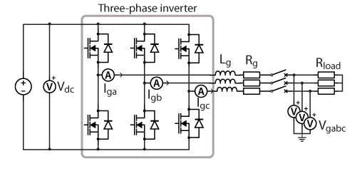
For the closed-loop control, the dq current control strategy is implemented. In this case, since the system is connected to a resistive load, the dq currents are expressed in the Laplace domain as shown in the equations below. Additionally, because the three-phase inverter does not need to be synchronized with the grid, a PLL is not required. Instead, the reference angle for the abc to dq0 and dq0 to abc transformations is generated using the angle generator block.
$$ \begin{aligned}[c] (1) \quad I_{g,d} = \frac{1}{(R_g+R_{load}) + s L_g} E_d + \omega_g L_g I_{g,q} \\ (2) \quad I_{g,q} = \frac{1}{(R_g +R_{load})+ s L_g} E_q – \omega_g L_g I_{g,d} \\ \end{aligned} $$
The closed-loop models of the three-phase inverter for Simulink and PLECS can be downloaded below:
Simulink models
PLECS models
To build the closed-loop control code and upload it to the controller, press Ctrl + B on Simulink (Ctrl + Alt + B on PLECS). This will automatically generate and compile the C code and launch Cockpit. This software facilitates experimental testing through various tools, such as scopes, rolling plots, and a transient generator. Additional details are provided in the Cockpit user guide.
After creating a new project, linking the user code with the controller, and setting the Cockpit workspace, the user can start running the control. For this, the next steps should be followed:
- Manually close the circuit breaker on the grid connection panel.
- To let power flow, close the relays of the grid connection panel by setting the variables
precharge_relayandbypass_relayto 1 in Cockpit. This validates that the corresponding GPO signals are properly wired. In this application, the precharge system could be bypassed; however, in a grid-connected system, this circuit must be connected properly to avoid high inrush currents. - Make sure that
ig_d_refandig_q_refare set to 0. - Gradually increase the DC supply voltage to 800V and check in Cockpit that
Vdcmatches the voltage of the DC source. If it does not, check that the sensor is connected to the correct analog channel and that its sensitivity is properly configured. - Enable the PWM pulses in the inverter stage by setting
activate_inverterto 1 and by toggling the PWM switch in the upper left corner in Cockpit. Theactivate_invertervariable activates the outputs of the CB-PWM blocks in the controller, while the switch enables the PWM signals. If either of these signals is set to 0, the PWM signals will be blocked. Further details about the CB-PWM block and the operation of the switch in Cockpit are available here and here, respectively. - Set
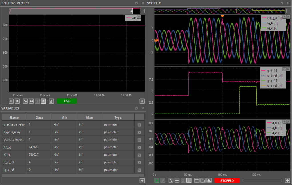
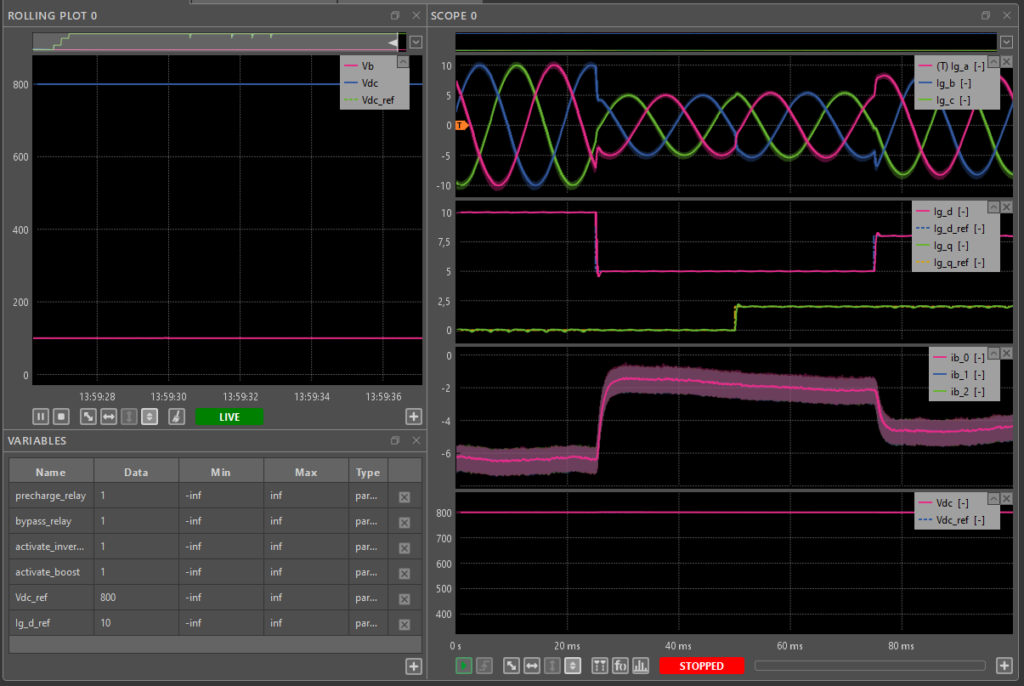
ig_d_ref= 1 and start increasing it gradually. Verify that the AC currentsIg_a,Ig_bandIg_care sinusoidal currents with fundamental amplitude equal to the value ofig_d_ref. - Set current steps using the transient generator. This allows the user to observe the transient response and, if necessary, adjust the controller parameters for better tuning. The results are shown in Fig. 5, where the following values have been assigned to the variables
id_refandig_q_ref:ig_d_ref= [4, 9, 7]Aatt= [0, 50, 100]sig_q_ref=[0, 6, 2]Aatt= [0, 125, 150]s
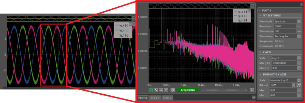
- To explore further possibilities inside Cockpit, use the spectral analyzer to examine the FFT spectrum of the generated currents with a current reference of
id_ref= 7. The obtained results are shown below:
- Set
id_refandiq_refto 0. - Deactivate the inverter by setting
activate_inverterto 0 and by disabling the PWM pulses with the switch in Cockpit. - Decrease the DC supply voltage to 0V and observe that the DC-link gets discharged (voltage
Vdcshould decrease to 0). - Open the bypass and precharge relays by setting
bypass_relayandprecharge_relayto 0.
Commissioning the closed-loop interleaved boost converter
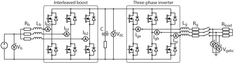
Commissioning the interleaved boost converter validates the correct operation and wiring of the other three power modules. The schematic and wiring of the system are depicted in the figures below. The converter is formed by connecting multiple boost converters in parallel. In this case, a resistive load of 500 Ω with a current rating of 1.6 A is used, connected to the DC bus.
The closed-loop control of the interleaved boost converter is implemented using a cascaded scheme, similar to that described in TN108. In this configuration, the outer loop regulates the DC bus voltage and is designed for perturbation rejection, while the inner loop provides current tracking, with one controller assigned to each leg. A phase-shifted switching method is used, similar to PN173, in which the switching instant of each leg is shifted by 1/n, where n is the total number of legs (in this case, three, resulting in a shift of 1/3). To improve measurement quality and provide an estimate of the period-averaged current independently from the sampling phase, synchronous averaging is applied to the ADC signals. A more complex alternative for cases where synchronous averaging is not available is presented in TN122.
The closed-loop model of the interleaved boost converter can be downloaded below:
Simulink models
PLECS models
After building the model, the user should create a new project and link the user code with the controller using Cockpit. Once this is done, the Cockpit workspace can be configured, and the user can start running the control following the next steps:
- Make sure that
activate_boostis set to 0 and that the PWM switch in Cockpit is deactivated, so that the converter remains inactive. - Set the DC supply voltage to 100V and check in Cockpit that
Vbindicates the same voltage. During this step, the DC bus will be precharged to approximately 100V. - Set
Vdc_ref= 200Vand enable the PWM pulses in the converter stage by settingactivate_boostto 1 and by toggling the PWM switch in the upper left corner in Cockpit.Vdcshould reach the reference value of 200V. - Increase
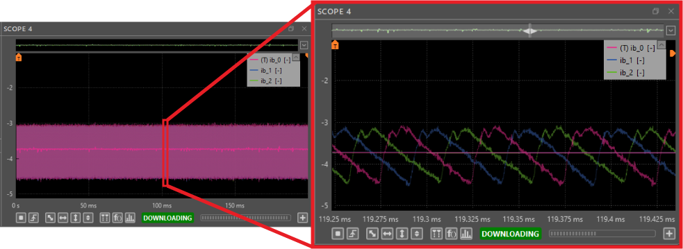
Vdc_refto700and verify that theVdcvoltage reaches the desired value. - Thanks to the oversampling capability of the B-Box 4, zooming in on the interleaved boost currents allows observing the ripple and the calculated average value obtained after synchronous averaging. This is illustrated below:
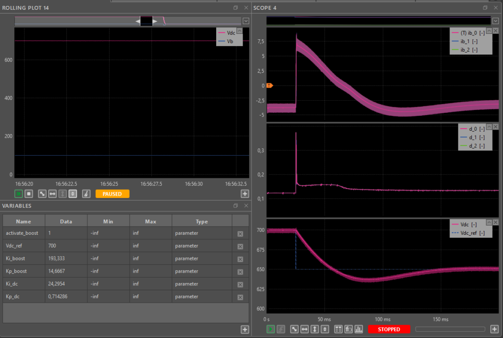
- Set a DC voltage step using the transient generator. This allows testing the transient response and, if necessary, adjusting the controller parameters. In this case, the DC voltage setpoint has been modified from 700V to 650V, with the corresponding results shown in Fig. 10. As can be observed, when the reference is changed, the current flowing through each leg of the interleaved boost is also modified.
- Deactivate the converter by setting
activate_boostto 0 and by disabling the PWM pulses with the switch in Cockpit. - Decrease the DC supply voltage to 0V and observe that
Vbdecreases to 0.
Commissioning the back-to-back system
Once the three-phase and the interleaved boost converter have been commissioned, all parts of the equipment have been tested and validated. Therefore, the back-to-back configuration can be implemented. For this setup, the system is configured as shown in the schematic of Fig. 1 and the system is wired as in Fig. 11. Three resistive loads of 11.5 Ω with a current rating of 10 A are implemented.
The previously described closed-loop control for the three-phase converter and the interleaved boost converter have been implemented in a single model to run the back-to-back example, in which the interleaved boost controls the common DC-bus voltage. Additionally, a feed-forward current term derived from the load side is included in the DC bus voltage control to improve dynamic performance.
The model of the back-to-back configuration for both Simulink and PLECS can be downloaded below:
Simulink models
PLECS models
After building the model, the user should create a new project and link the user code with the controller using Cockpit.
Finally, the Cockpit workspace can be configured and the user can start the final test following these steps:
- Make sure that the circuit breaker on the grid connection panel is closed.
- To let power flow, close the relays of the grid connection panel by setting the variables
precharge_relayandbypass_relayto 1 in Cockpit. The wiring has been previously tested when commissioning the three-phase inverter. - Make sure that
ig_d_refandig_q_refare set to 0. - Gradually increase the DC supply voltage to 100V and check in Cockpit that
Vbmatches the voltage of the source. During this step, the DC bus will be precharged to approximately 100V. - Make sure that
Vdc_refis higher than 100V. - Enable the PWM pulses in the interleaved boost by setting
activate_inverterto 1 and by toggling the PWM switch in the upper left corner in Cockpit. Observe thatVdcincreases until reaching the reference voltage valueVdc_ref. - Increase gradually the DC link voltage reference to 800V (
Vdc_ref = 800V). - At this point, the DC bus is already charged. Then, the three-phase converter PWM signals can be enabled. To do so, set
activate_boostto 1. - Set
ig_d_ref= 1 and start increasing it gradually. Verify that the AC currentsIg_a,Ig_bandIg_care sinusoidal currents with fundamental amplitude equal to the value ofig_d_ref. - Set current steps using the transient generator. This allows observing the transient response and, if necessary, adjusting the controller parameters. The following values can typically be assigned to the variables
id_refandiq_ref:id_ref= [10, 5, 8] Aatt= [0, 25, 75]msiq_ref=[0, 2]Aatt= [0, 50]ms
The results are shown in Fig. 12. As shown, the grid currents accurately track their references. When a step is applied to grid current references, the power demanded by the system changes. Since Vb remains constant, this change in power is reflected in the interleaved boost currents through the feed-forward term, which increases or decreases the current accordingly. Finally, as the DC voltage controller has been tuned for perturbation rejection, it can be observed that the DC voltage remains minimally impacted by this disturbance.
- Set
ig_d_refandig_q_refto 0. - Deactivate the inverters by disabling the PWM pulses with the switch in Cockpit and by setting
activate_inverterandactivate boostto 0. - Decrease the DC supply voltage to 0V and observe that
Vbdecreases to 0 and that the DC-link gets discharged. - Open the bypass and precharge relays by setting
bypass_relayandprecharge_relayto 0.
Going further
For further reading, AN006 presents a similar topology, but including connection to the AC grid.