Table of Contents
This page is a quick-start guide to build an interleaved boost converter using imperix equipment. It is specifically made to accompany users who want to get familiar with imperix’s solutions and build their first converter with the B-Box 4 using the Simulink or PLECS blockset. The converter is built using imperix power modules and the passive filter box.
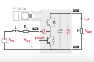
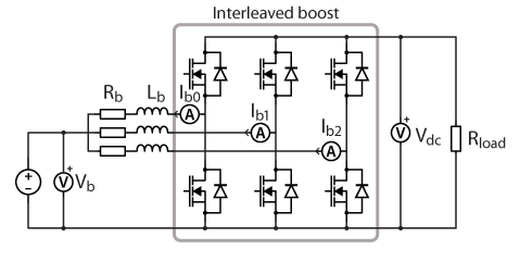
The guide focuses on implementing an interleaved boost converter connected to a resistive load on the high-voltage side. The topology is shown in Fig. 1. In this configuration, three legs are interleaved to reduce ripple and distribute current; nevertheless, the topology is scalable and additional legs can be incorporated if higher power requirements are needed. The basic working principles of a single-leg boost converter, which can be extended to the interleaved boost, are explained in TN101.
Required hardware equipment
The individual components required to build the interleaved boost converter are given below. The list comprises imperix products as well as additional components commonly available in research laboratories:
- Imperix products:
- 1x programmable controller (e.g. B-Box 4)
- 3x half-bridge modules
- 1x passives filters box
- Control development tools for Simulink and PLECS (ACG SDK), with a valid license
- 1x external VSR-1000-ISO.
- Others:
- 1x load resistor (see sizing below)
- A DC power supply
- Safety laboratory cables (banana)
- Optional: voltage and current probes with an oscilloscope
Passive components sizing
The system uses a 500Ω resistor rated for 1.6A as the resistive load, which is compliant with the 700V DC bus voltage rating. This corresponds to about 1kW of power. If the user wishes to operate at higher power, a resistor with a higher power rating should be used. More details regarding the sizing of passive components are given in TN101.
Building and wiring the interleaved boost converter
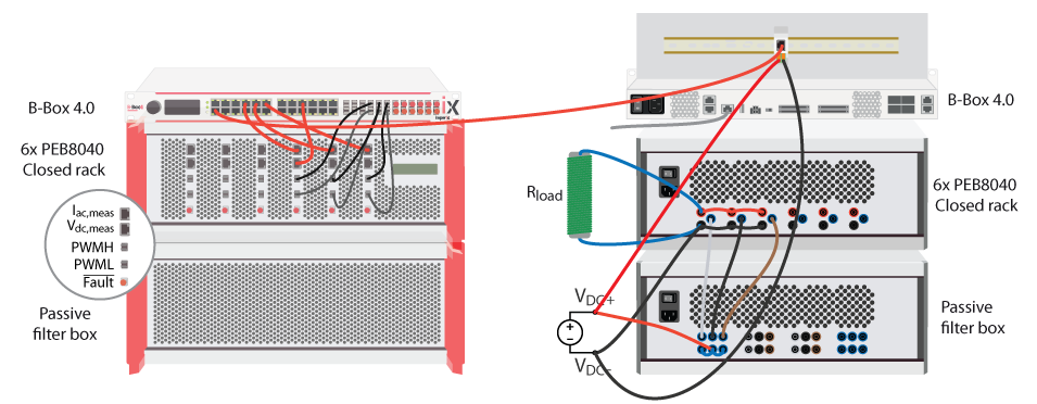
The wiring of the system is executed as shown in Fig. 2. The main points to consider are as follows:
- The Ethernet cable is connected to the back of the B-Box 4 so that it can be interfaced from Cockpit. More information on connecting to the controller is available in PN138.
- Ensure each optical fiber is matched with its designated module and channel.
- The sensors are connected to the designated analog inputs of the controller. Further details on configuring the analog I/Os are provided in the next section.
- The midpoint of the modules is connected to the inductors.
- The DC source is correctly connected by linking DC+ to the outputs of the inductors, connected in star configuration, and DC− to VDC− of the modules (see Fig.2).
- The DC buses of the modules are interconnected and connected to the external resistor.
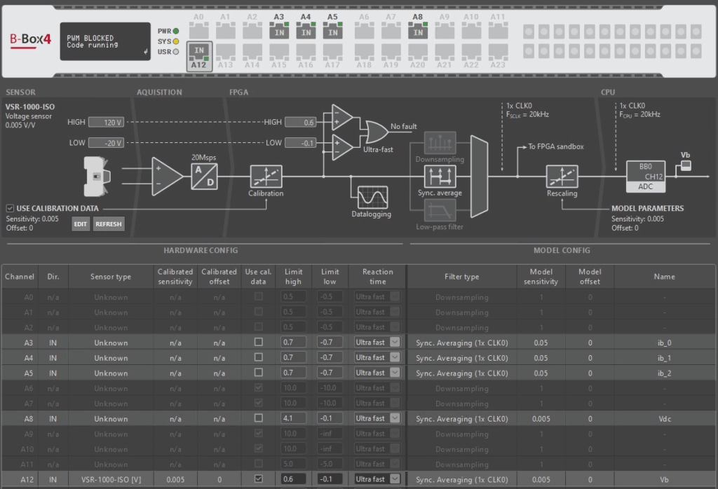
Analog input configuration
Before doing any experiments, it is essential to properly configure the analog input channels of the B-Box 4. These channels have both hardware and software settings. The hardware settings can be configured from Cockpit or the B-Box 4 front panel, and the software settings are configured inside the Simulink or PLECS control model.
Software settings
- Channel number
- Sensor type
- Sensitivity and offset
- Sampling strategy
Hardware settings
- Protection reaction time (e.g. over-current or over-voltage detection)
- Safety limits (upper and lower thresholds)
- For auto-identified sensors: model parameters or sensor calibration data
More information about the ADC block of Simulink and PLECS blocksets can be found here. Additionally, related information on the analog I/O configuration on B-Box 4 can be found in PN252.
For the channel to which an external VSR-1000-ISO sensor is connected, the B-Box 4 automatically detects the sensor. The user can then choose to use the calibration data stored in the sensor’s EEPROM. More information about sensor auto-configuration is provided in PN255.
The analog channels have been configured as shown in Fig. 3. The limits were computed with a safety margin to prevent undesirable tripping. In this case, no offset was detected. However, if an offset is observed on any channel (i.e., the measured value is different from zero when no signal is applied), the offset should be adjusted. This can be done through the ADC block or, for auto-identified sensors, via Cockpit. More information about sensor calibration is provided in document PN255.
Software
Two pieces of software are required to develop the B-Box control code: the imperix Automated Code Generation Software Development Kit (ACG SDK), which can be downloaded here; and a compatible version of Matlab (2016 and newer) or PLECS.
A detailed guide on how to set up the software can be found in PN133.
Creation of the Simulink model
The control model below implements open-loop output-current control, with step-by-step instructions for creating it provided afterwards. The implementation of a closed-loop current control is given in PN171.
In this example, interleaved operation is used, meaning that the switching instant of each leg is shifted by 1/n, where n is the total number of legs (in this case, three, resulting in a shift of 1/3). This reduces the amplitude of the current ripple while simultaneously augmenting the apparent switching frequency (of the interleaved boost) by a factor of n.
To effectively reject the ripple in all three current measurements , synchronous averaging is applied to the ADC signals over exactly one PWM period. This automatically computes the averaged value of the indivial currents, although the carriers – and hence current ripples – are phase-shifted. For reference, without oversampling, significantly more complex sampling strategies are required, notably such as presented in TN122.
The open-loop model of the interleaved boost converter for Simulink and PLECS can be downloaded below. More information on how to create a Simulink or PLECS model are given in PN134 and PN136, respectively.
Simulink models
PLECS models
Real time execution of the interleaved boost converter
The code can be built by pressing Ctrl + B on Simulink (Ctrl + Alt + B on PLECS). This will automatically generate and compile the C code that will be uploaded to the B-Box 4. Pressing Ctrl + B also launches the Cockpit monitoring software. Additional details are avialable in the Cockpit – User guide.
After creating a new project and linking the user code with the controller, the user can set up the Cockpit workspace as in the following example:
- Two different scopes are added to the scope module. The first one will include the three measured currents (
Ib_0,Ib_1,Ib_2) and the second one the applied duty cycles (d_a, d_b, d_c). - The DC bus voltage (
Vdc) and the low-voltage side boost voltage (Vb) are added to a rolling plot. - The
Dvariable is added to the variables module.
Once the workspace has been set, the next steps can be followed to run the control software:
- Make sure that PWM switching is disabled in Cockpit (project pane, upper-left in Cockpit), so that the converter remains inactive at first.
- Gradually increase the DC supply voltage to 100V and check in Cockpit that
Vbmatches the DC source voltage. If it does not, check that the sensor is connected to the correct analog channel and that its sensitivity is properly configured. During this step, the DC bus will be precharged to approximately 100V. - Set the duty cycle variable
Dto 0.5. This corresponds to an output voltageVdcthat is twice the input voltageVb, namely 200V. - Enable the PWM pulses in the inverter stage by toggling the PWM switching in the upper left corner of Cockpit. The DC bus voltage should rise to roughly 200 V. Due to the diode voltage drop and other non-idealities, it does not reach the theoretical value predicted by \(V_{dc} = \frac{V_b}{1-D}\). A change in the duty cycle will result in a corresponding change in the DC bus voltage.
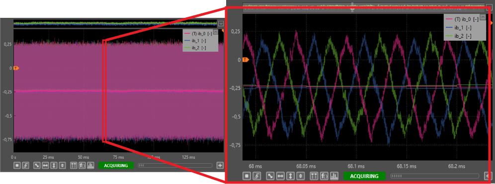
- Verify that the boost currents
Ib_0,Ib_1andIb_2are constant currents with amplitude $${I_b}=\frac{V_{b}}{3R_{load}}(\frac{1}{1-D})^2\ \ (\approx 0.25\,\text A).$$ Since the current flows from the low-voltage side to the high-voltage side, it is considered negative. Thanks to the oversampling feature of the B-Box 4, by zooming in on the interleaved boost current scope, the current ripple can be observed, as well as the calculated average value of \(−0.25 \,\text{A}\) obtained after synchronous averaging. This is illustrated in Fig. 4
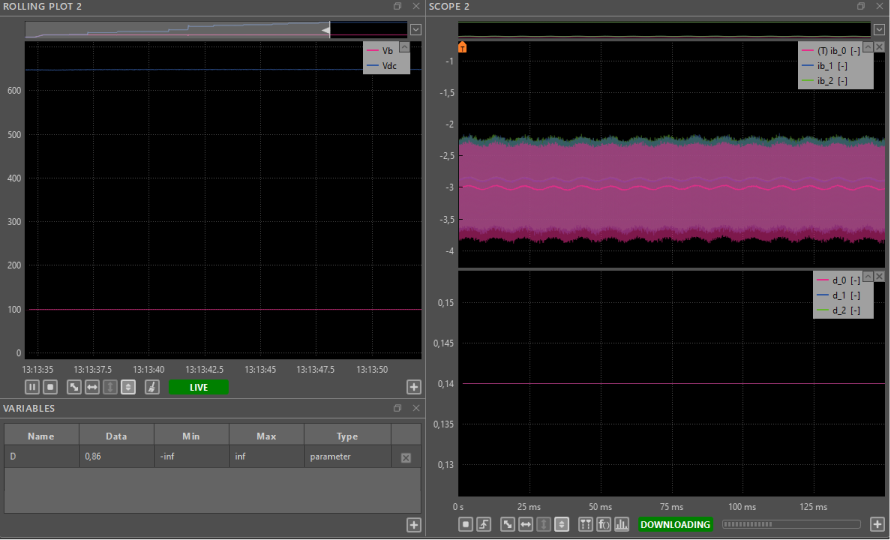
- Gradually increase
Dto 0.86. The steady state results under these conditions are shown in Fig. 5.
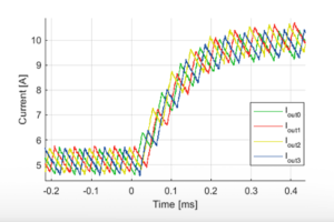
- Generate steps in the duty cycle by using the transient generator located in the right-hand panel. At
t=50ms,Dis modified from 0.45 to 0.6. This step will result in a higher DC bus voltage. In addition, as the required power increases during the transient andVbkeeps constant, the current through each leg of the interleaved boost will also increase. The obtained results can be observed in Fig. 6.

- Deactivate the inverter by disabling the PWM pulses with the switch in Cockpit.
- Decrease the DC supply voltage to \(0\,\text{V}\) and and observe that
Vbdecreases to 0.
Going further
An alternative sampling configuration, for cases where synchronous averaging is not available, is presented in the interleaved buck converter note. On the other hand, for a more complex application where the interleaved boost is set in a back-to-back configuration with a three-phase inverter, the reader is redirected to PN171.