Table of Contents
This technical note describes the operating principles of a step-up boost converter. A possible open-loop control implementation of this converter, targeting the B-Box RCP or B-Board PRO with both C/C++ and automated code generation approaches, as well as experimental results are presented.
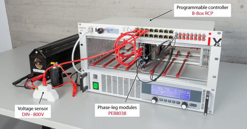
(Power supply and passive components not sold by imperix)
What is a step-up boost converter?
A step-down buck converter is a type of DC to DC switched-mode power converter like the Step-down buck converter and the Buck-boost converter. Made from two semiconductors (a transistor and a diode), an inductor, a capacitor, and a load resistor, this converter steps up the input voltage \(V_{in}\) to a higher output voltage \(V_{out}\) according to [1]. By switching on and off \(S_1\), the inductor current increases and decreases. The magnitude of these current ripples depends on the input voltage, the duty cycle \(D\), the inductor \(L\) and the switching frequency \(f_{sw}\) of the transistor. This current will then charge the output capacitor, which accumulates the energy transferred from the inductor.
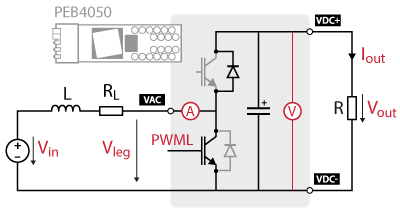
The schematic below presents the topology of a boost (step-up) converter.
The well known input to output voltage relation for a boost converter follows the equation
$$V_{out} = V_{in} * \frac{1}{1-D}$$
Continuous and discontinuous conduction
Similar to the buck converter, the boost converter can also operate in continuous and discontinuous conduction mode, depending on the inductor current. For more information on the conduction modes, please refer to the Step-down buck converter note. Also, a plot of the operating mode boundaries can be found in [2].
Boost converter implementation with imperix power modules
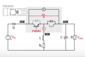
Since imperix power modules are based on bidirectional switching cells, the boost converter implementation is very similar to the one of the buck. In a sense, the boost is just a buck whose input and output have been reversed. Note that there is no need for an external output capacitance since it is already integrated into the power module.
IGBT switching cell
Therefore, the same considerations on semiconductor technology can be applied to the boost. This means that, when using IGBT modules, only the low-side transistor is driven.
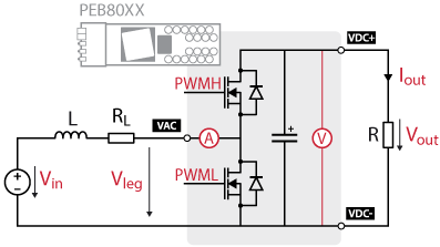
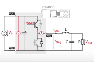
MOSFET switching cell
With MOSFETs, however, both transistors are driven for synchronous rectification. The page Step-down buck converter further details the difference of implementation between both technologies.
Effect of parasitic components
A specific characteristic of the boost converter is the impact of the parasitic components of the circuit, specifically the inductor’s parasitic resistance \(R_L\), illustrated above. Adding this series resistance to the model, the relation between the input and output voltage becomes $$V_{out} = V_{in}*\frac{1}{1-D}\frac{1}{1+\frac{R_L}{R(1-D)^2}}$$
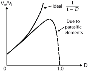
This much more complex relation hints that a small parasitic resistance will have a significant impact on the circuit behavior. Indeed, the graph below shows the difference in normalized output voltage for both scenarios (ideal and non-ideal).
To give an idea, with an 8.5 [Ω] load resistor and a 0.1 [Ω] inductance resistance, the maximum \(V_{out}/V_{in}\) ratio is 4.6 and is located at a duty cycle of 0.89. However, one should still be careful when doing experiments since the output voltage can nonetheless go very high.
Sizing the passive components
The switching of the transistors induces ripples in the inductor current and the output voltage. The current ripples’ amplitude \(\Delta I_{L}\) is determined by the following equation:
$$ \Delta I_{L} = V_{in} \frac{D}{Lf_{sw}}$$
and the voltage ripple’s amplitude follows:
$$ \Delta V_{out} = V_{in} \frac{D}{RCf_{sw}(1-D)}.$$
Defining an acceptable value for the ripple’s amplitude for a given input voltage, frequency and duty cycle allows for the computation of the passive components.
For instance, with an input voltage of 100 [V], an output voltage of 150[V], and a frequency of 20 [kHz], using an off-the-shelf inductor of 2.36 [mH], the current ripple would have a magnitude of \(\Delta I_{out} =0.71\) [A]. Adding an output capacitance of 2 [mF] and a resistor of 100 [Ω] would then result in an output voltage ripple magnitude of \(\Delta V_{out} =12.5 \)[mV].
Academic references
[1] Mohan, Undeland, Robbins: “Power Electronics”, 2002
[2] P. Barrade: “Switched-mode converters (one quadrant)“, 2006
B-Box / B-Board implementation
Software resources
Simulink model
PLECS model
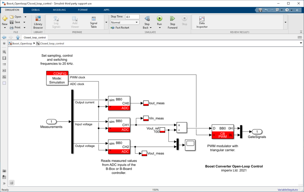
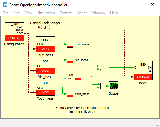
The provided Simulinkand PLECS models implement a simple open-loop control for the step-up converter using the ACG SDK for simulation and code generation. The duty cycle of the PWM signals is computed by dividing the measured input voltage by the desired reference output voltage in a feedforward fashion. The figures below show an overview of the algorithm implementation on Simulink and PLECS.
Experimental results
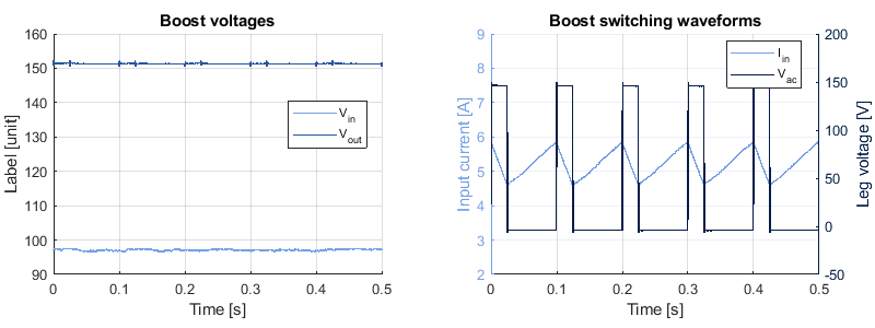
The two following plots present the expected experimental behavior of a step-up (boost) converter. In this operating point (D = 1/3), the converter steps up the input voltage from 100 [V] to 150 [V]. The right plot shows the input current ripples, as well as the leg voltage \(V_{leg}\).
