Table of Contents
To implement power converter control algorithms in an FPGA, it is often required to develop an FPGA-based pulse-width modulation (PWM) module. Therefore, this note presents how to implement a custom PWM modulator in the Xilinx FPGA of the imperix controller (B-Box RCP or B-Board PRO).
The presented modulator uses FPGA pulse-width modulation with a triangular carrier. The sources of this example can be re-used in an FPGA-based power converter control design. Alternatively, it can be used as a starting point to develop more complex custom PWM modulators.
The first section of this page explains how the PWM module fits into an FPGA-based control design as well as the FPGA design of the pulse-width modulation. Next, the actual implementation of the FPGA modulator is presented using 3 different tools:
- the Xilinx blockset for Simulink System Generator
- the Simulink add-on MATLAB HDL Coder
- hand-written VHDL coding
Then, a Simulink testbench is built to test the FPGA design in simulation. Finally, the modulator is integrated into the imperix controller FPGA to be validated.
For most use-cases, using CPU-based control and the pre-implemented carrier-based PWM modulators of the imperix library is widely sufficient and should be preferred.
Design choices for the FPGA-based PWM modulator
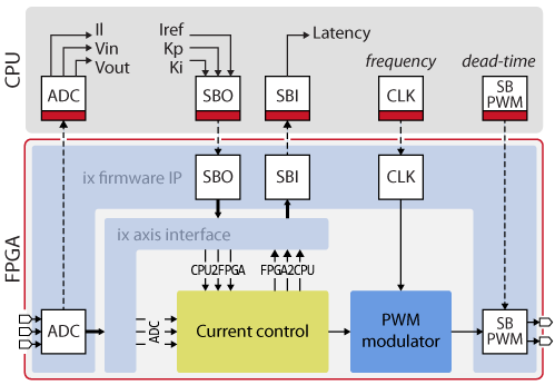
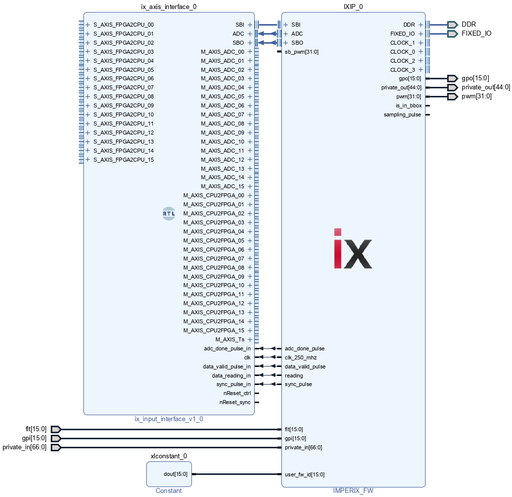
The Pulse Width Modulator (PWM) is intended to be used in a larger design such as the FPGA-based buck converter control example shown in the image below. The imperix firmware IP and ix axis interface are explained in the getting started with FPGA control page and the current control module is presented in the high level synthesis for FPGA tutorial.
The FPGA-based PWM modulator must be connected to one of the 4 clock generators (CLK). In this example, the CLK allows synchronizing the CPU control task with the PWM carrier. For further details on the CLK FPGA signals, please refer to the “CLOCK interface” section of imperix firmware IP user guide.
The Sandbox PWM (SB-PWM) block makes it possible to drive the same PWM output chain as that used by other modulators (CB-PWM, PP-PWM, DO-PWM, and SS-PWM). This allows the user to generate complementary signals with dead-time, use the standard activate and deactivate functions and rely on the protection mechanism that blocks PWM outputs when a fault is detected.
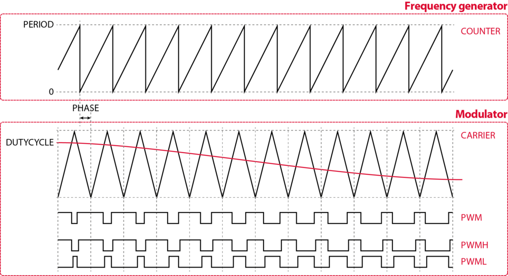
The figure below shows how the FPGA modulator operates. The pulse-width modulation is obtained by comparing a duty cycle value with the triangular carrier wave.
The duty cycle can be updated using a single rate or double rate. When using the single-rate update, the duty cycle value is applied when the triangular carrier reaches its minimum. With the double-rate update, the duty cycle is updated twice per period: when the carrier reaches its maximum and when it reaches its minimum.
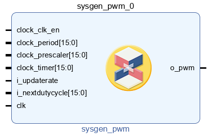
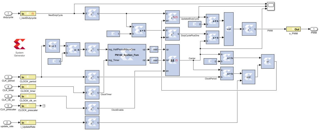
The FPGA-based PWM module is shown below. The screenshot shows the IP generated with System Generator (now called Vitis Model Composer HDL blockset), but the input and output ports are identical when using MATLAB HDL Coder or VHDL. The ports are the following:
CLOCK: the clock interface that is meant to be connected to the CLOCK output of imperix firmware IP. It contains:CLOCK_prescaler, the CLK_timer ticking rate, 1 tick = (4 ns/CLK_prescaler)CLOCK_clk_en, asserted to indicate a new tick.CLOCK_period, the PWM period in ticksCLOCK_timer, a counter that goes from 0 to CLK_period-1
next_dutycycle: the next duty cycle to be updated. This signal is a 16-bit unsigned integer with a unit of ticks.update_rate: controls the update rate. ‘0’ is single-rate and ‘1’ is double-rate.pwm: the pulse-width modulation output signal
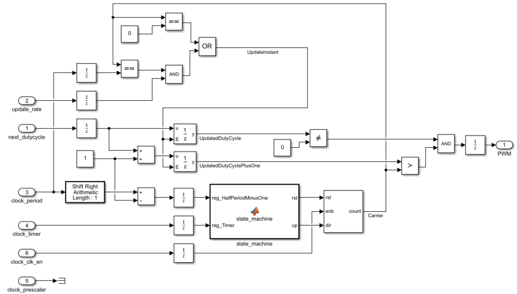
Below is shown the high-level schematic of the FPGA-implemented PWM modulator. The duty cycle is stored in a register, whose enable port is controlled by the update rate. The triangular carrier is generated from the CLOCK input using an up/down counter that behaves as follows:
- it resets each time CLOCK_timer is equal to zero
- after a reset, it counts UP until CLOCK_timer reaches CLOCK_period/2
- then, it counts down until it reaches zero.
How to implement pulse-width modulation in FPGA?
This section provides 3 possible approaches for implementing the FPGA PWM modulator, using Xilinx System Generator, MATLAB Simulink HDL Coder, or hand-written VHDL.
1) FPGA PWM using Xilinx System Generator
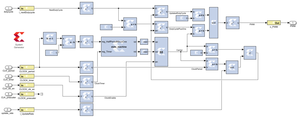
The implementation of the FPGA PWM modulator using Xilinx System Generator is given below. The sources are available on the System Generator introduction page.
Please note the following important points:
- The input and output ports are represented with Gateway in and Gateway out blocks. The sample time is set to 4ns to ensure that the model represents the real behavior of the FPGA.
- All the input signals are registered to improve performance.
- In System Generator, users can configure the latency for each block. If there is a timing violation in the generated IP, try to increase the latency or insert registers between operations.
- The carrier is generated using a free-running counter and a state machine that controls the counter. System Generator provides MCode block where users can convert MATLAB code to VHDL. The MATLAB code for the state machine is given below.
function [up,rst] = state_machine(reg_HalfPeriodMinusOne, reg_Timer)
persistent state, state = xl_state(0,{xlUnsigned, 1, 0});

% default value
up = 1;
rst = 0;

switch state
  case 0 % counting up
    up = 1;
    rst = 0;
    if reg_Timer > reg_HalfPeriodMinusOne
      state = 1;
    end
  case 1 % counting down
    up = 0;
    if reg_Timer == 0
      state = 0;
      rst = 1;
    else
      rst = 0;
    end
endCode language: Matlab (matlab)
2) FPGA PWM using HDL Coder
The implementation of the FPGA PWM modulator using HDL Coder is given above. The sources are available on the MATLAB HDL Coder introduction page.
Please note the following important points:
- The input and output ports are represented with Simulink input and output ports. The sample time is set to 4ns to ensure the model represents the real behavior in FPGA.
- The delay block can be used to represent the register in FPGA.
- The carrier is generated using a free-running counter and a state machine that controls the counter. Here, the state machine is implemented using a MATLAB Function block. The MATLAB code for the state machine is given below.
function [rst, up] = state_machine(reg_HalfPeriodMinusOne, reg_Timer)

% define states
state_up = uint8(0);
state_down = uint8(1);
persistent state
if isempty(state)
  state = state_up;
end

% default value
up = true;
rst = false;

switch state

  case state_up % counting up
    up = true;
    rst = false;
    if reg_Timer > reg_HalfPeriodMinusOne
      state = state_down;
    end

  case state_down % counting down
    up = false;
    if reg_Timer == 0
      state = state_up;
      rst = true;
    else
      rst = false;
    end
end
Code language: Matlab (matlab)
3) FPGA PWM using VHDL
The following VHDL code implements the FPGA pulse-width modulation design but in hand-written VHDL.
Testing the FPGA-based PWM module in simulation
The following test bench is used to validate the proper functioning of the FPGA pulse-width modulation with a Simulink simulation. The screenshots below show the test of PWM using the Xilinx System Generator implementation, but the testbench is identical for testing the MATLAB HDL Coder implementation.
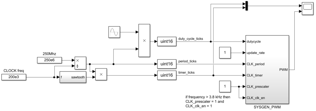
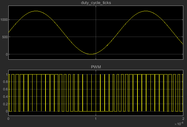
The testbench generates CLOCK signals that are identical to the interface of the imperix firmware IP. The CLOCK frequency is set to 200 kHz. A sinusoidal signal ranging from 0 to CLOCK_period (in ticks) is connected to the dutycycle input. The following plot validates that the resulting PWM has a frequency of 200 kHz and that its duty cycle varies from 0 to 1 following the sinusoid.
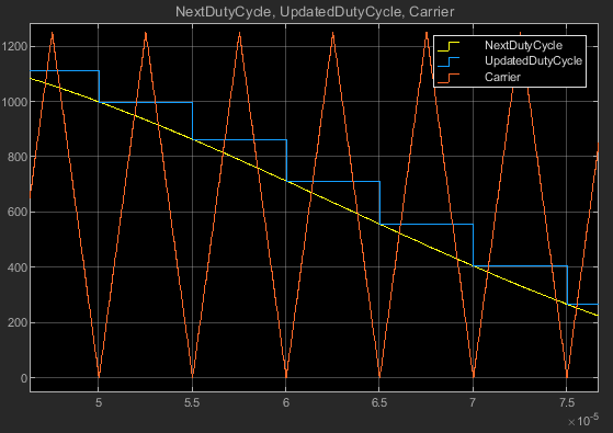
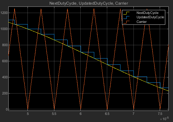
As shown below, the behavior of internal signals of the PWM module can also be inspected by adding scopes inside the Xilinx System Generator design. System Generator will complain and show red (!). It does not cause any problem during simulation but it is important to remove any scope before generating the FPGA IP.
The internal signal UpdatedDutyCycle is the actual value compared to the triangular carrier to generate the PWM signal. Changing the constant signal applied to the update_rate input allows selecting between single-rate update (0) and double-rate update (1). These two modes are documented in the standard carrier-based PWM block help. Observing internal signals allows checking that the UpdatedDutyCycle behaves according to the selected update rate mode.
Integrating the PWM modulator into the Xilinx FPGA
Description of the FPGA-based PWM modulator example
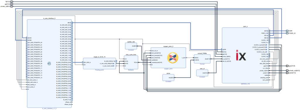
The FPGA design illustrated below is used to test the generated FPGA PWM modulator. Its purpose is to manually select the duty cycle of the modulator from a PC by using Imperix Cockpit. To do so, a tunable parameter block is used on the CPU. It is configured with the name duty_cycle and the data type single. This value is transferred from the CPU to the FPGA using the CPU2FPGA_00 interface (SBO_00 and SBO_01) as explained in the getting started with FPGA control page. In the FPGA, this single-precision duty-cycle is transformed into an integer value in ticks as follow:
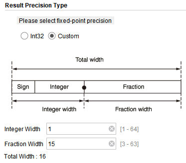
- The 32-bit single-precision floating-point value is transformed into a 16-bit fixed-point value with an integer width of 1-bit and a fraction width of 15-bit (fix16_15). This repartition has been chosen because the duty cycle is expected to range between 0.0 and 1.0 so only 1-bit is required on the integer part.
- To obtain a value in ticks, the result of the previous step is multiplied by CLOCK_period. The result of the multiplication of a fix16_15 with a uint16 is a fix32_15 (32-bit, 17-bit integer part, and 15-bit fractional part).
- Finally, only the 16 first bits of this result are used as the duty cycle input of the FPGA PWM modulator IP.
The CLOCK_0 will be used as a clock reference for the FPGA pulse-width modulation, which means that the PWM modulator will run at the same frequency as the CPU control task and that both will stay synchronized. (That is because the CPU interrupt rate is always defined by CLOCK_0.)
On the imperix firmware IP, the sb_pwm[31:0] port provides access to the same PWM output chain as that used by other modulators (CB-PWM, PP-PWM, DO-PWM and SS-PWM). This allows the user to generate complementary signals with dead-time, use the standard activate and deactivate functions and rely on the protection mechanism that blocks PWM outputs when a fault is detected.

sb_pwm input (sb_pwm[0], sb_pwm[2], sb_pwm[4], etc.). Another example of such a configuration is available in the FPGA-based hysteresis current control examplepwm port, as this would bypass the enable/disable mechanism! Instead, the SB-PWM driver is meant to provide proper access to PWM outputs, which should be used in all cases. This is critical since this mechanism also handles fault management!CPU-side implementation
As with any FPGA-based implementation, a CPU code is still required to configure the imperix IP and define real-time variables accessible from the various Cockpit modules. In the current example, the CPU code
- configures the frequency of CLOCK_0,
- configures the Sandbox PWM driver,
- declares the
duty_cyclevariable and transmits it to the FPGA through the SBO interface.
Using ACG SDK on Simulink
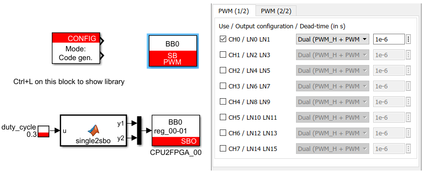
The frequency of CLOCK_0 is defined in the Configuration block, and the duty_cycle (float) variable is created using a tunable parameter block. It is then mapped to M_AXIS_CPU2_FPGA_00 using the the MATLAB Function block single2sbo (as introduced in Getting started with FPGA control development).
The SB-PWM block is used to configure and activate/deactivate the output PWM channel 0 (CH0) (lane #0 and lane #1). The output is configured as Dual (PWM_H + PWM_L) with a deadtime of 1 µs. This configuration expects a PWM signal coming to sb_pwm[0] input of the imperix firmware IP and will automatically generate the complementary signals with the configured deadtime.
Using CPP SDK
The equivalent functionalities can also be implemented in C code, using CPP SDK. The corresponding code is available for download below.
FPGA-side implementation using Vivado
The TN141_vivado_design.pdf file below shows the full Vivado FPGA design. Here are the step-by-step instructions to reproduce it.
- Create an FPGA control implementation starter template by following the Getting started with FPGA control implementation.
- Add the FPGA PWM IP into your Vivado project. System Generator is taken as an example but the steps are identical for a VHDL or an HDL Coder module.
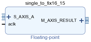
- Add a Floating-point IP and select the Float-to-fixed operation. Select Single precision for input and Integer Width 1, Fraction Width 15 (fix16_15) for output. This module will convert the duty cycle sent by CPU from single to fix16_15.
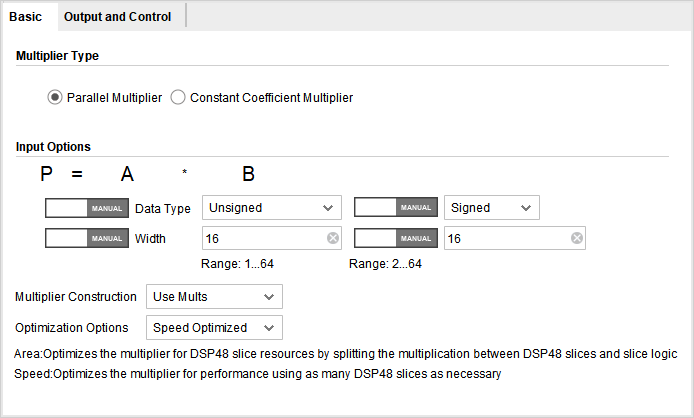
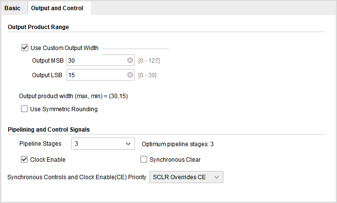
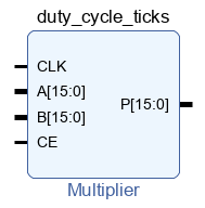
- Add a Multiplier IP and set the configuration as shown below.
- The input A is connected to the
CLOCK_periodso it is set to 16-bit unsigned - The input B is connected to the fixed-point duty cycle so it is set to 16-bit signed
- The output range is set to return only the 16 first bits of the integer part of the result
- The clock enable (CE) input is enabled and will be connected to the tvalid output of the single_to_fix16_15 IP output. This way, the multiplication is performed synchronously with the data coming from the AXI4-Stream.
- The input A is connected to the
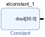
- Add a Constant IP to set all the 31 unused
sb_pwmoutputs to ‘0’. Set its Const Width to 31 and its Const Val to 0.
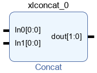
- Add a Concat IP. It will serve to concat the pwm output of the PWM IP with the zeros of the Constant IP.
- Connect the pins as follows:
- all the CLOCK_0 signals of the imperix firmware IP signals to the PWM block
- M_AXIS_CPU2FPGA_00 to S_AXIS_A of single_to_fix16_15
- CLOCK_0_period to A of the Multiplier
- tdata of M_AXIS_RESULT of single_to_fix16_15 to B of the Multiplier
- tvalid of M_AXIS_RESULT of single_to_fix16_15 to CE of the Multiplier
- P of the Multiplier to i_nextdutycycle
- o_pwm of the PWM IP to In0 of the Concat IP
- dout of the 31-bit to zero Constant IP to In1 of the Concat IP
- dout of the Concat IP to the sb_pwm input of the imperix firmware IP
- all the IP clocks to clk_250_mhz
And finally, the design can be synthesized and the bitstream generated:
- Click Generate bitstream. It will launch the synthesis, implementation and bitstream generation
- Once the bitstream generation is completed, click on File → Export → Export Bitstream File… to save the bitstream somewhere on your computer.
Experimental validation
The bitstream can be generated and loaded into the device using Cockpit, as explained in the Getting started with FPGA control implementation page. Then, the Simulink model TN141_CPU_side.slx can be built and launched as explained in the Programming and operating imperix controllers getting started page.
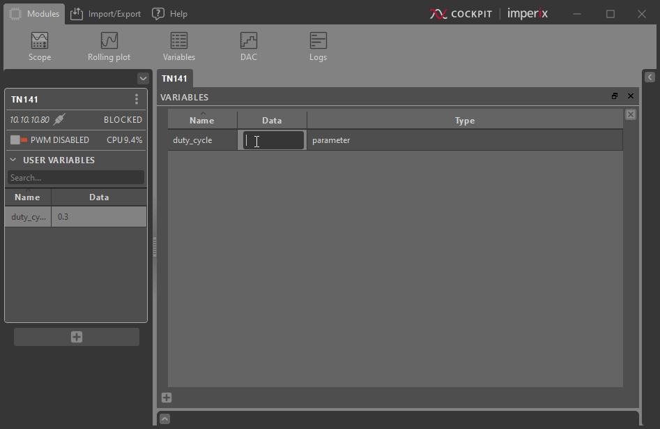
Using the Variables module of Cockpit, the duty_cycle variable can be changed in real-time. After enabling the PWM outputs, the PWM signals at the output CH0 (lanes 0 & 1) can be observed using an oscilloscope or a logic analyzer.
The screenshot below shows the measured PWM signals using a logic analyzer, as expected the measured signals are complementary 50 kHz PWM signal with a duty cycle of 30% and a dead time of 1 µs.
Going further
The high-level synthesis for FPGA developments page re-uses this FPGA PWM modulator in a PI-based current control of a buck converter scenario. It shows how to integrate and connect HLS-generated IPs in a realistic FPGA power converter control implementation.


