Table of Contents
This technical note describes the operating principles of a buck-boost converter. A possible open-loop control implementation of this converter, targeting the B-Box RCP or B-Board PRO with both C/C++ and automated code generation approaches, as well as experimental results are presented.
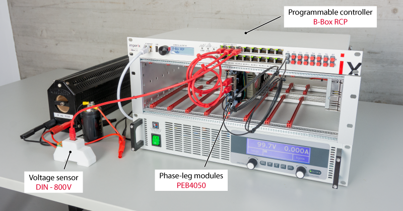
(Passive components and power supply not sold by imperix)
What is a buck-boost converter?
A step-down buck converter is a type of DC to DC switched-mode power converter like the Step-down buck converter and the Step-up boost converter. It can be considered as the combination of a buck and a boost converter since it is able to step down and step up the input voltage according to [1]. In an ideal buck-boost converter, the output voltage ranges from 0 to \(\infty\). The specificity of this converter is the inverted polarity of the output voltage.
The converter’s schematic is presented below.
The input to output voltage relation for a buck-boost converter is described by the following equation: $$V_{out} = -\frac{D}{1-D} V_{in}$$
The minus sign on the equation’s left side explains the inverting property.
Continuous and discontinuous conduction mode
Similar to the buck and boost converter, the buck-boost converter can also operate in continuous and discontinuous conduction mode, depending on the inductor current. For more information on the conduction modes please refer to the Step-down buck converter note. Also, a plot of the operating mode boundaries can be found in [2].
Buck-boost converter implementation with imperix power modules
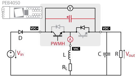
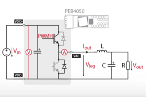
The implementation of the converter using imperix’s power modules is illustrated by the schematic below.
Only the high side IGBT is driven in this case. However, if a MOSFET power module is used, it is recommended to drive both transistors for synchronous rectification. This subject is further detailed in Step-down buck converter.
Note that the power module’s capacitor, highlighted in red on the schematic, is connected between \(V_{in}\) and \(V_{out}\). This capacitor does not affect the correct behavior of the circuit. However, several practical details are to be kept in mind when doing experiments.
First, since the output voltage polarity is inverted, the voltage across the module’s capacitor is \(V_{in} – V_{out} = V_{in} + |V_{out}|\). The designer should then be careful not to exceed the maximum DC bus voltage rating. Second, a protection diode should be placed after the power supply. Indeed, when the converter is turned off, the output voltage goes back to zero. Since the VDC+ terminal of the module is floating, its voltage will rise to V_{in} + |V_{out}| resulting in potential reverse current flow in the power supply.
Last but not least, if a polarized capacitor is used at the output, make sure to connect it in the correct way, meaning the plus terminal to ground, since the output voltage polarity is inverted!
Effect of parasitic components
Having similar characteristics to the boost, the buck-boost also suffers from non-idealities [2]. Taking the inductor’s parasitics resistance into acount, the new transfer function becomes: $$V_{out} = -V_{in}* \frac{D}{1-D} \frac{1}{1+\frac{R_L}{R(1-D)^2}} $$
For more information, please look at the Step-up boost converter.
Passive component selection
The switching of the transistors induces inductor current and output voltage ripples. The current ripples’ amplitude \(\Delta I_{L}\) are determined by the following equation: $$ \Delta I_{L} = V_{in} \frac{D}{Lf_{sw}}$$
The voltage ripple’s amplitude follows the equation: $$ \Delta V_{out} = V_{in} \frac{D^2}{RCf_{sw}(1-D)}$$
Defining an acceptable value for the ripple’s amplitude, for a given input voltage, frequency, and duty cycle allows for the computation of the passive components.
For instance, with an input voltage of 100 [V], an output voltage of 150[V], and a frequency of 20 [kHz], using an off-the-shelf inductor of 2.36 [mH], the current ripple would have a magnitude of \(\Delta I_{out} = 1.27\) [A]. Adding an output capacitance of 2 [mF] and a resistor of 60[Ω] would then result in an output voltage ripple magnitude of \(\Delta V_{out} = 37.5\) [mV].
Academic Reference
[1] Mohan, Undeland, Robbins: “Power Electronics”, 2002
[2] Texas Instrument: “Understanding Inverting Buck-Boost Power Stages in Switch Mode Power Supplies“, Application Report SLVA059B, March 1999 revised March 2019
B-Box and B-Board implementation
Software resources
Simulink model
PLECS model
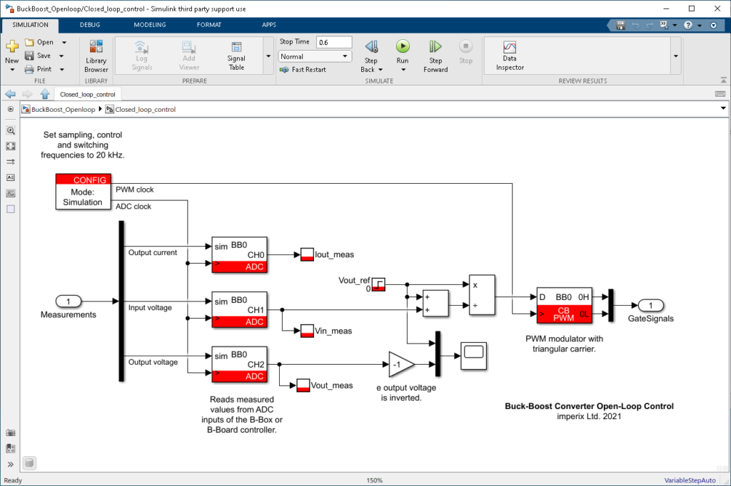
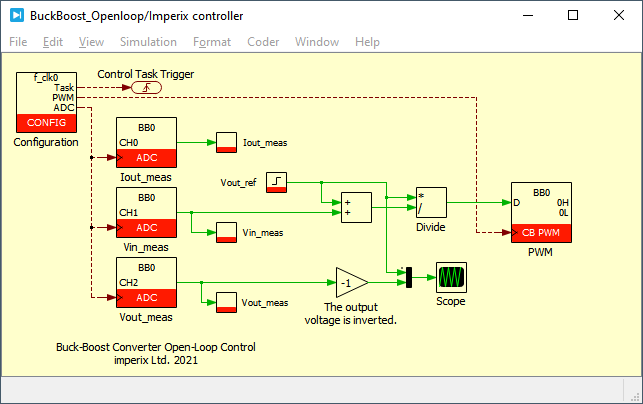
The provided Simulink and PLECS model implements a simple open-loop control for the converter using the ACG SDK for simulation and code generation. Isolating the duty cycle from the aforementioned CCM transfer function gives $$ D = \frac{V_{out}}{V_{out}-V_{in}}$$ The duty cycle for the PWM is then computed with the measured input voltage and the reference output voltage, in a feedforward fashion. The figure below shows an overview of the Simulink algorithm.
Experimental results
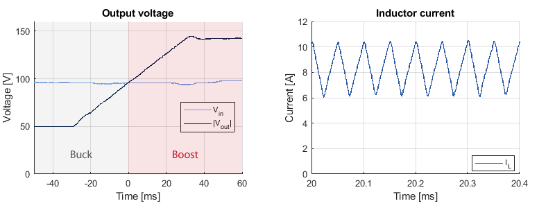
The two following plots show the voltage step-up and step-down capabilities of the buck-boost converter as well as the inductor current ripples. The buck-boost is, in this case, able to change its output voltage from -50 [V] to -150 [V]. Note that the absolute value of the output voltage is plotted here.
The perturbation seen on the input voltage is most probably due to oscillations in the circuit since it is operating in open-loop. Also, the output voltage in boost mode does not fully reach 150 [V] due to the parasitic resistance of the inductor, as previously explained.


