Table of Contents
This technical note describes the operating principles of a step-down buck converter. A possible open-loop control implementation of this converter, targeting the B-Box RCP or B-Board PRO with both C/C++ and automated code generation approaches, as well as experimental results are presented.
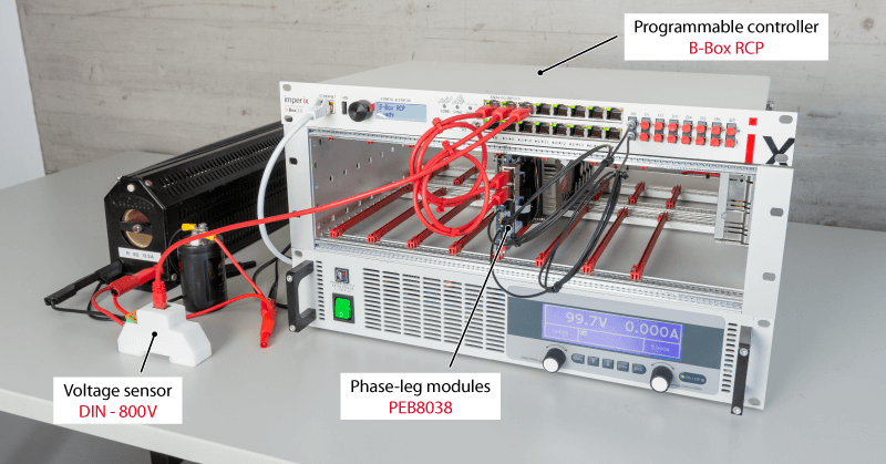
(Power supply and passive components not sold by imperix)
What is a step-down buck converter?
A step-down buck converter is a type of DC to DC switched-mode power converter like the Step-up boost converter and the Buck-boost converter. Made from two semiconductors (a transistor and a diode), an inductor, and a load resistor, this DC/DC converter steps down the input voltage \(V_{in}\) to a lower output voltage \(V_{out}\) according to [1]. The well-known relation between input and output voltage in a buck converter is: $$V_{out} = D * V_{in}$$
The circuit topology is shown in the figure below.
By switching on and off \(S_1\), the inductor current increases and decreases. The magnitude of these current ripples depends on the input voltage, the duty cycle \(D\), the inductor \(L\) and the switching frequency \(f_{sw}\) of the transistor. A filter capacitor is then placed in parallel to the load resistor to reduce the ripples on the output voltage.
Note that, for systems with higher power requirements, it is possible to parallel several switching cells to build an interleaved buck converter. Benefits, tradeoffs and controls strategies for interleaved converters are all addressed in the aforementioned page.
Continuous and discontinuous conduction
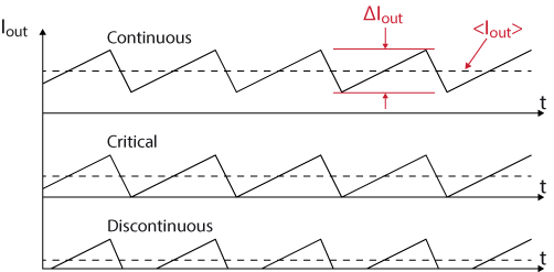
Depending on the operating conditions the output current of the step-down buck converter can vary significantly. As shown in the graph below, when the average output current is close to zero, the diode D1 clips the negative parts of the ripples. This does not happen with higher output currents.
Two operating modes can then be distinguished depending on the inductor current. If it is always higher than zero, the converter is in Continuous Conduction Mode (CCM). Conversely, if this current drops to zero the step-down converter is said to operate in Discontinuous Conduction Mode (DCM).
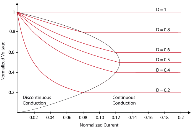
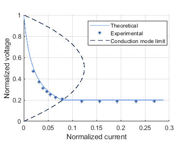
The buck converter’s operating condition can be visualized on the graph below when considering the normalized voltage (\(V_{out}/V_{in}\)) and normalized current (\(I_{out}Lf_{sw}/(V_{in})\)). In a more intuitive way, the step-down converter is in the discontinuous mode for low load currents and in continuous mode in the opposite case.
As suggested by the previous plot, the relation between input and output voltage is linear in CCM (\(V_{out} = D*V_{in}\)). However, in DCM, the discontinuities in the current result in a much more complex, non-linear input to output voltage relation.
Buck converter implementation with imperix power modules
The implementation of the converter with imperix power modules is based on a bidirectional switching cell (two switches with anti-parallel diodes). Therefore, depending on the semiconductor technology, the operation of a step-down buck can slightly vary. For imperix’s power modules, two device technologies are available: IGBTs and MOSFETs.
IGBT switching cell
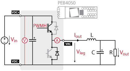
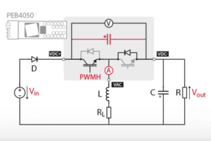
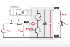
Using an IGBT power module, like the PEB4050 (or legacy PEB8032 and PEB4046), as a switching cell, the implemented circuit’s schematic is presented below.
The bottom IGBT is not switched and is only used for its antiparallel diode. This circuit can very well be used in both CCM and DCM.
MOSFET switching cell
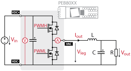
Using a MOSFET power module, like the PEB8038 or the PEB8024, as a switching cell, the implemented circuit’s schematic is presented below.
In this case, since MOSFET’s body diodes perform poorly, significant losses will be dissipated when the upper switch is open.
To avoid this issue, reverse conduction of the bottom MOSFET is generally used instead. Indeed, using a PWM signal to drive the low-side transistor as well, the current will go through the channel of the transistor and not the body diode. This technique, called synchronous rectification, therefore improves the efficiency of the buck converter.
Note that with synchronous rectification, the converter can only operate in CCM, since the current can flow in both directions in the bottom MOSFET.
Sizing the passive components
The switching of the transistors induces current and thus voltage ripples in the output stage. The current ripples’ amplitude \(\Delta I_{out}\) is determined by the following equation:
$$ \Delta I_{out} = V_{in} \frac{D(1-D)}{Lf_{sw}}$$
The voltage ripple’s amplitude follows the equation:
$$\Delta V_{out} = V_{in} \frac{D(1-D)}{8 L C f_{sw}^2}$$
Defining an acceptable value for the ripple’s amplitude for a given input voltage, frequency, and duty cycle allows sizing the passive components.
For instance, with an input voltage of 100 [V], an output voltage of 20 [V], and a frequency of 20 [kHz], using an off-the-shelf inductor of 2.36 [mH], the current ripple would have a magnitude of \(\Delta I_{out} = 0.34\) [A]. Adding an output capacitance of 2 [mF] would then result in an output voltage ripple magnitude of \(\Delta V_{out} = 1\) [mV].
Academic references
[1] Shepherd, William and Zhang, Li; “Power Converter Circuits”; 2004
[2] P. Barrade; “Switched-mode converters (one quadrant)“; 2006
B-Box / B-Board implementation
Software resources
Simulink model
PLECS model
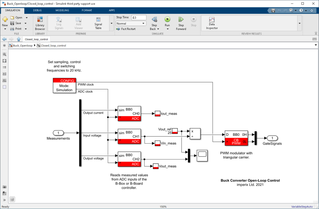
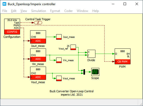
The provided Simulink and PLECS model implement a simple open-loop control for the step-down buck converter using the ACG SDK for simulation and code generation. The converter is assumed to be operating in CCM. The duty cycle of the PWM signals is then computed by dividing the desired reference output voltage by the measured input voltage in a feedforward fashion. The figures below show an overview of the algorithm implementation on Simulink and PLECS.
Experimental results
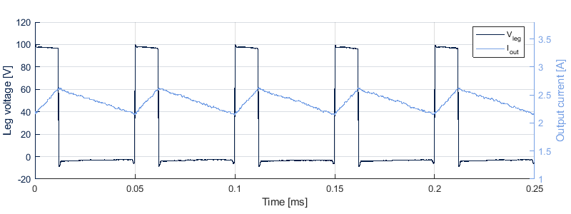
The current ripples along with the leg voltage \(V_{leg}\) were experimentally measured when stepping down a voltage of 100 [V] to 20 [V]. As expected, the output current rises when the switch is turned on and falls during the off-state.
Also, measurements of the normalized current and voltage were performed at different frequencies to experimentally confirm the conduction mode theory.
The experimental results at a duty cycle of 0.2 show an excellent agreement with the theoretical values.


