Table of Contents
This page presents a method for selecting an inductance value for a Dual Active Bridge (DAB) isolated DC-DC converter. DAB converters can be easily constructed with four imperix half-bridge modules (PEB series) or with two full-bridge modules (PEH series). Proper inductor selection can greatly increase the efficiency of the DAB converter by minimizing semiconductor losses.
Parameters definition
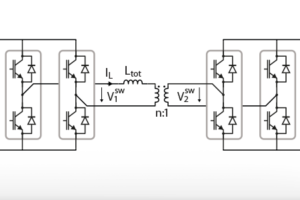
The DAB converter is a popular choice among DC-DC converters due to its galvanically isolated nature, bidirectional power flow, and high efficiency under the correct operation [4]. The following figure shows the circuit of an unloaded DAB converter:
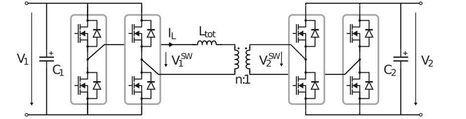
The rest of the page will refer to V1, V2, and n as defined above. In addition, phase shift control detailed extensively in DAB modulation techniques is assumed to be the chosen control method for this converter. The converter is assumed to have DC buses on both sides, not a resistive load. Before selecting an inductance value, it is important to know the desired operating conditions and specifications of the DAB converter. These values are defined as follows:
| Parameter | Definition |
|---|---|
| Maximum Power [W] | Maximum rated power for converter operation |
| Minimum Power [W] | Minimum power desired for converter operation |
| V1 [V] | Input Voltage |
| V2 [V] | Output Voltage |
| fsw [Hz] | Switching frequency (actual switching frequency of a single switch and carrier frequency is fsw/2) |
| ∆TPWM [s] | The time resolution of the PWM generator (for the imperix B-Box RCP this is 4 ns) |
| n | Transformer turns ratio (as defined above) |
| ∆Pmax [W] | The maximum allowable change in power flow when the minimum adjustment to the control variable (phase shift) is made |
| ∆ϕmin=fsw*∆TPWM | The minimum possible adjustment of phase shift (depends on time resoltion of digital controller) |
When selecting a transformer turns ratio n, it greatly increases the efficiency of phase-shift control to choose n such that V1=nV2. However, when operating with a wide voltage range or constrained by available components, this is not always possible.
It is important to note that Ltot refers to the sum of the leakage inductance and any external inductance placed before the transformer as referenced from the primary side of the converter. This page will offer a methodology for selecting a value for Ltot but when choosing an external inductor component, it is important to take the leakage inductance of the selected transformer into account as well.
Minimum inductance for ZVS
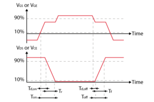
Semiconductor switching can be a significant source of power loss in a switched-mode power supply such as a DAB converter. Turn-on switching losses are typically much more significant than turn-off losses and occur when a FET has a nonzero voltage and nonzero current for some period during turn-on [3].
The use of dead-time between complementary PWM signals in the DAB converter (each leg of both full bridges are complementary in phase-shift modulation) not only serves to avoid shoot-through current, but also facilitate zero voltage switching (ZVS). The operation of the converter in the ZVS region eliminates turn-on losses. During dead-time, the switch that was previously on has been turned off and the switch about to be turned on has not been yet. The inductor current discharges the drain-to-source capacitance of the FET so that when the switch is turned on, zero voltage has been reached across the switch that is about to be turned on.
In order to achieve ZVS in the DAB converter, the energy stored in Ltot when one full-bridge switches (IL will be at its peak in phase shift modulation) must be sufficient to discharge the energy stored in the drain-source capacitances of the FETs that are about to be turned on and charge the drain-source capacitance of the FETs that have just been turned off [1]:
$$\frac{1}{2}L_{tot}I_{pk}^2>2C_{oss}V_1^2$$
Where Coss is the datasheet value for FET output capacitance and Coss ≈ Cds. Note that this is an approximation due to the inherent nonlinearity of Coss. Based on this inequality, it follows that:
$$L_{tot,min}>\frac{4C_{oss}V_1^2}{I_{pk}^2}$$
where:
$$I_{pk}=\frac{T_s}{4L_{tot}}\left(V_1+(4\phi-1)nV_2\right)$$
and for P<Pmax:
$$\phi=\frac{1}{4}\cdot\left(1-\sqrt{1-\frac{8f_{sw}L_{tot}|P|}{nV_1V_2}}\right).$$
Solving for L sets a minimum value for Ltot, as defined above, so that the DAB converter operates in the ZVS region. This value should be calculated using the minimum desired operating power so that the converter will achieve ZVS across all power levels.
Minimum inductance for power resolution requirement
The RMS current flowing through the inductor, transformer, and switches at a given power level increases with inductance value Ltot, therefore, it would seem to make logical sense to select inductance value Ltot.min calculated from the previous section so as to stay in the ZVS region but avoid unnecessary conduction losses due to an increase in RMS currents. However, there are several reasons not to do this.
First, it is preferable to overdesign L by some margin due to non-idealities that appear in a physical converter that are ignored in simulation and/or theory. For example, the presence of dead times and parasitic capacitances within the printed circuit board (PCB) will increase the required inductance value for operating within the ZVS region.
Second, considering the equation for power transfer [in Watts] of a DAB converter with phase-shift control (note that ϕ refers to a phase shift between 0 and 1 as a proportion of switching period):
$$P(\phi)=\frac{nV_1V_2}{f_{sw}L_{tot}}\phi(1-2\phi)$$
For a given power level, a smaller selected inductance value, Ltot will lead to a smaller required phase shift value, phi. Because power transfer has a nonlinear (inverted parabolic) correlation with phi, the smaller the value selected for phi is, the larger the change in power flow will be when phi is adjusted by the controller. Assuming a digital controller of some type, there will be a minimum possible adjustment in phase shift (defined above), which will lead to a minimum change in power with each adjustment of phi by the controller. This can be quite large at low values of Ltot, leading to undesirably large steady-state oscillations in the power flow of the converter. Therefore, it is important to define the maximum tolerable ∆P (as defined above) and design Ltot based on the following constraint:
$$\Delta P=P(\phi_2)-P(\phi_1)<\Delta P_{max}$$
where
$$\phi_2=\phi_1+\Delta \phi_{min}.$$
One way of solving this is with a short script that increments Ltot starting from Ltot,min calculated in the previous section, until ∆P is less than the desired power resolution ∆Pmax.
The resulting minimum Ltot value needed to meet the resolution requirements at a given power level should be compared to the previously calculated minimum value to achieve ZVS and the larger chosen as Ltot,min so as to meet both sets of design constraints. This quantity should be selected using the minimum power value desired to operate the converter at. If the design meets the maximum resolution requirement at minimum power, it will exceed the requirement at maximum power.
Maximum inductance for required power transfer
Considering again the equation for power transfer of a DAB converter with phase shift control, it is seen that, for a given set of operating conditions and a fixed value of Ltot, there will be a maximum power level achievable (at ϕ = 0.25). Therefore, when designing for Ltot, it is important that the inductance value is small enough to reach the maximum power specification. To address this, the aforementioned equation can be rewritten as:
$$L_{tot,max}=\frac{nV_1V_2}{8f_{sw}P_{max}}$$
This adds an upper design constraint to the choice of inductance value for the DAB converter.
Inductor Selection
After completing the initial calculations above, the final inductance value can be selected for the DAB converter. As demonstrated in the previous sections, selecting a value for Ltot between Ltot,min and Ltot,max should assure that the DAB converter can reach maximum rated power while still achieving ZVS and adequate power resolution at the minimum operating power. For most applications, the final choice of inductor should be some percentage greater than Ltot,min so as not to incur switching losses, but substantially less than Ltot,max to not unnecessarily increase the RMS currents in the switches. The final choice of inductor will depend on component availability, converter layout choices, transformer characteristics, and application specifics. This will ultimately be a tradeoff between power control resolution and RMS currents.
In the case that Ltot,min exceeds Ltot,max, the desired operating conditions cannot be met and the specifications considered in the first section should be modified in order to achieve desirable converter operating conditions. This may include adjusting the switching frequency or the transformer turns ratio. Alternative control schemes may be considered as well, such as triangular or trapezoidal modulation, which is out of the scope of this article.
To better illustrate the tradeoff between power control resolution and RMS currents, and help select an appropriate inductance, the following Matlab script can be used.
Other Considerations
The methodology outlined above is a simple, first-pass design procedure. Various factors that may merit consideration and adjustment in the inductance value include, but are not limited to, the effect of dead-time on converter operation, nonlinear device capacitances, transformer parasitics, and PCB layout. The effect of dead-time on converter operation must be considered more carefully at high-frequency, low-power converter operation [1].
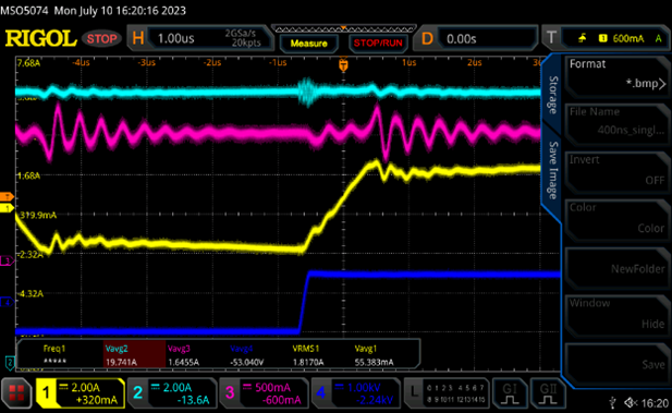
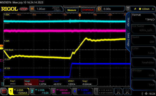
In order to minimize the effects of the parasitic capacitance of the transformers, the inductance value Ltot can be split into two and placed on each leg of the primary side of the capacitance so that the switched node is not directly connected to the transformer. This can also be done on each leg of both sides of the transformer (4 total inductors) but the inductance value must be scaled across the transformer turns ratio n by a factor of n2. The significant difference in the oscillations of the input current (light blue), output current (pink), and inductor current (yellow) between split and single inductors can be seen in the following two figures.
Further in-depth information on DAB converter operation, design, and control can be found in [1] and [2] and on the imperix knowledge base.
References
[1] Costinett, Daniel Jesse. “Analysis and Design of High Efficiency, High Conversion Ratio, Dc-dc Power Converters,” Ph.D. Dissertation, University of Colorado Boulder, 2013.
[2] F. Krismer, “Modeling and Optimization of Bidirectional Dual Active Bridge DC-DC Converter Topologies,” Ph.D. dissertation, ETH Zurich, 2010.
[3] X. Li, L. Zhang, S. Guo, Y. Lei, A. Q. Huang and B. Zhang, “Understanding switching losses in SiC MOSFET: Toward lossless switching,” 2015 IEEE 3rd Workshop on Wide Bandgap Power Devices and Applications (WiPDA), Blacksburg, VA, USA, 2015, pp. 257-262.
[4] L. Li, G. Xu, D. Sha, Y. Liu, Y. Sun and M. Su, “Review of Dual-Active-Bridge Converters With Topological Modifications,” in IEEE Transactions on Power Electronics, vol. 38, no. 7, pp. 9046-9076, July 2023.