Table of Contents
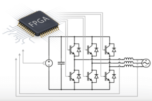
This note presents an FPGA control implementation of a grid-tied current-controlled inverter. It combines several control modules presented in different Technical Notes to form a complete converter control, executed entirely in the FPGA of a B-Box RCP controller.
Thanks to the FPGA programmability of the B-Box controller, complex control algorithms can be effectively executed at high rates and with minimal latency. In particular, this example shows that a grid-oriented current control algorithm can be executed as fast as 650 kHz, whereas the equivalent CPU-based execution is “limited” to 210 kHz (which is already an industry-leading figure amongst prototyping controllers).
Besides, the fast switching frequency used in this example takes full advantage of the imperix SiC phase leg module.
Grid-tied inverter control
The controlled system is a standard current-controlled voltage-source inverter, connected to a 3-phase grid. This converter is built using imperix power modules in the experimental validation section.
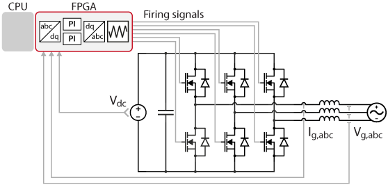
The control algorithm is entirely executed in the controller FPGA and implements a three-phase PLL for grid synchronization coupled to a standard dq current control in the grid-oriented reference frame. Based on user-defined current references, the controller computes the voltages that the inverter should produce in order to match the required current. These voltages are then modulated in PWM signals and fed to the gates of the inverter.
The overall inverter control algorithm is shown below, and each of the elementary control blocks is further described in the following sections.
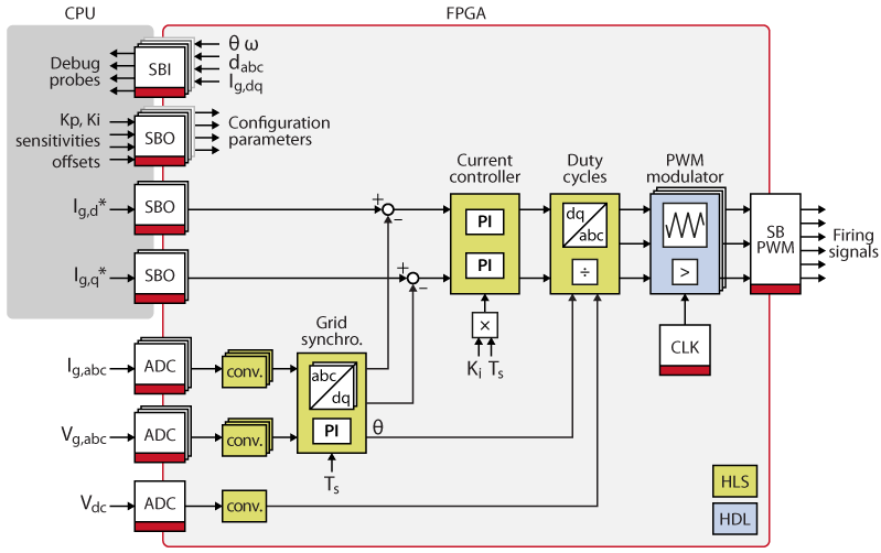
Overview of the FPGA-based inverter control task
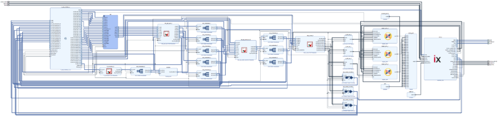
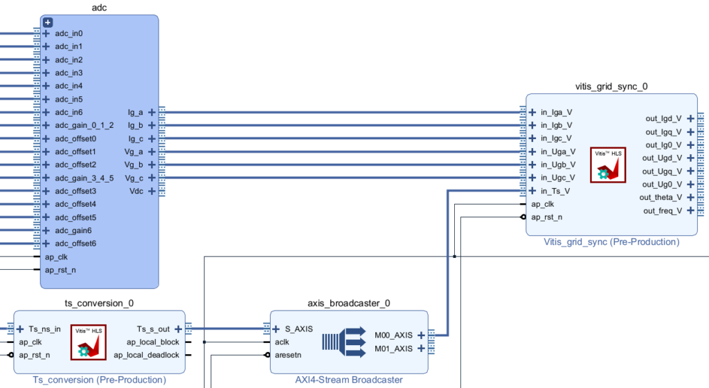
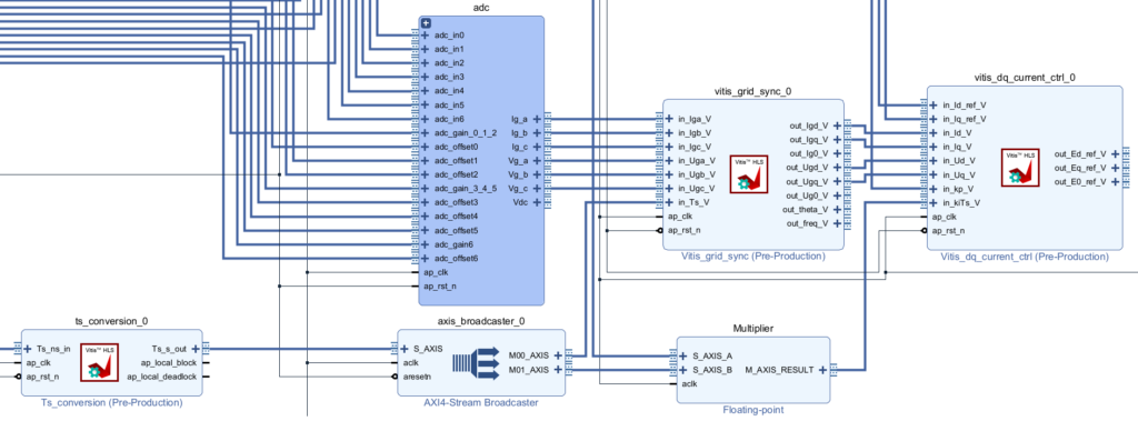
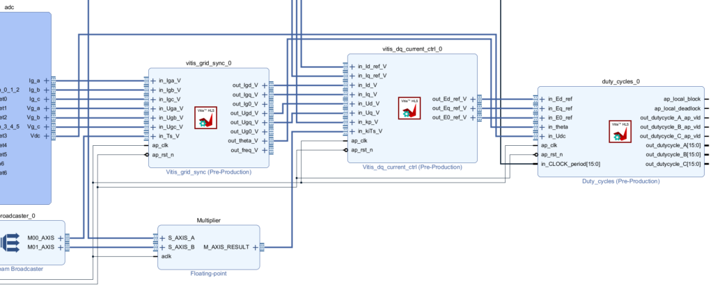
Below is shown the implemented Vivado block design used to generate the FPGA bitstream. The creation of the Vivado block design section describes in more detail how to reproduce this block design. All the sources can be downloaded by clicking on the button below.
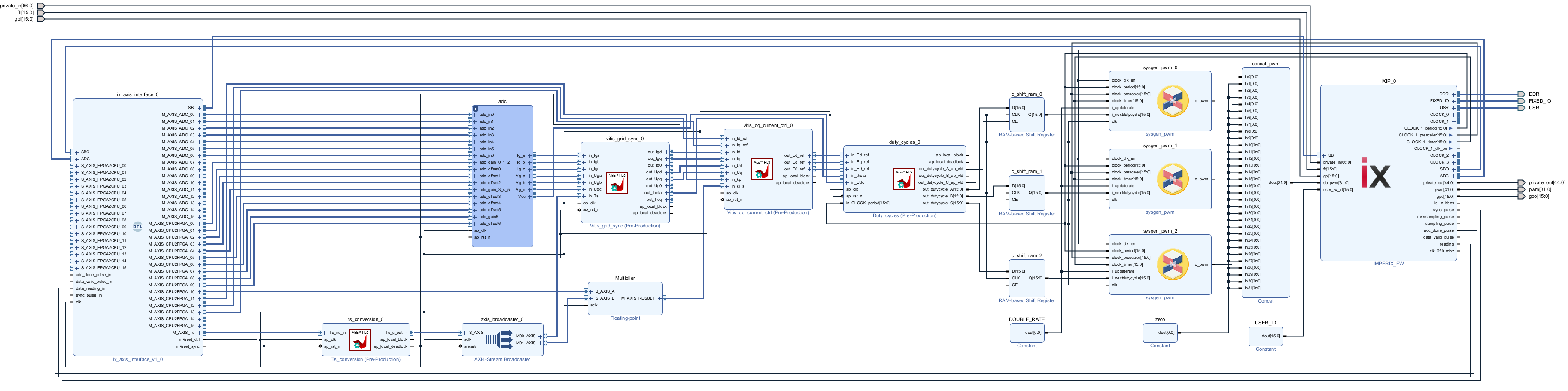
The design uses the following IPs
- ADC conversion module (Vitis HLS)
- Ts conversion module (Vitis HLS)
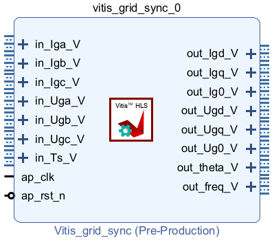
- Grid synchronization module (Vitis HLS or Model Composer, documented in TN143)
- Dq current controller (Vitis HLS or Model Composer, documented in TN144)
- duty cycle computation module (Vitis HLS)
- Carrier-based PWM module (System Generator or HDL Coder, documented in TN141)
These IPs have been implemented using High-Level Synthesis tools such as Vitis HLS (free of cost, C++) and Model Composer (~500$, requires MATLAB Simulink). These tools offer a simple yet powerful way of developing control algorithms in FPGA.
Performance analysis of the control task
Without any special optimization, the latency of the presented inverter control algorithm is roughly 1.5µs (see details below), which means that it can run above 650 kHz. Comparatively, the similar CPU-based algorithm presented in TN106 can run at up to 210 kHz.
Latency and control delay
The total latency can be estimated by simply adding up the latency of each module, which are:
Module | Latency Vitis HLS | Latency Model Composer |
|---|---|---|
| ADC conversion | 24 cycles | 24 cycles |
| Grid synchronization | 145 cycles | 146 cycles |
| DQ current control | 72 cycles | 56 cycles |
| Duty cycles computation | 138 cycles | 137 cycles |
| Total latency | 379 cycles (1.52µs) | 363 cycles (1.45µs) |
That estimated latency is comparable to the measured latency of 385 cycles (1.54µs) with the Vitis HLS implementation. The Model Composer approach achieves a slightly lower latency thanks to automatic optimization but at the expense of slightly higher resource utilization.
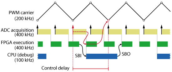
Considering a conversion time of the ADC chip of 2µs, the total control delay is 3.54µs, which is larger than one sampling period (chosen 2.5µs – 400kHz). Therefore, the execution of the control task is pipelined with the ADC acquisition, as shown in the figure below. The control delay to consider when tuning the current controller is therefore \(T_{d,ctrl}=2T_{s}\).
Further details on control delay identification can be found in the PN142.
Controller tuning
The gains of the PI controllers are tuned using the Magnitude Optimum, as introduced in Vector current control. The total delay of the control loop is identified as:
- Control delay: \(T_{d,ctrl}=2T_{s}=5\,\text{µs}\)
- Modulator delay (double-rate update): \(T_{d,\text{PWM}}=T_{sw}/4=T_{s}/2=1.25\,\text{µs}\)
- Sensing delay: (16 kHz filter) \(T_{d,sens}\approx 10\,\text{µs}\)
- Total loop delay: \(T_{d,tot}=T_{d,ctrl}+T_{d,\text{PWM}}+T_{d,sens}\approx 16.25\,\text{µs}\)
Resource utilization
The resource utilization is estimated by Vivado after the implementation and is shown below, for the Vitis HLS approach.
Resource | Utilization (inverter control) | Utilization (imperix firmware 3.6) | Total utilization |
|---|---|---|---|
| LUT | 18’733 | 24’220 | 42’953 (54.65%) |
| LUTRAM | 115 | 798 | 913 (3.43%) |
| FF | 30’713 | 50’732 | 81’445 (51.81%) |
| BRAM | 2 | 37 | 39 (14.72%) |
| DSP | 104 | 0 | 104 (26%) |
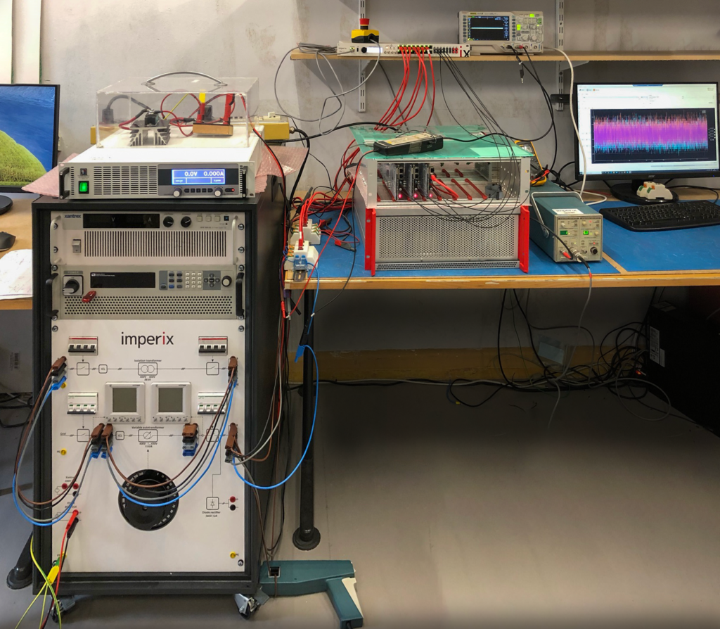
Experimental validation
Testbench description
A physical testbench is built to validate the developed control strategy experimentally, using the following equipment:
- Controller: B-Box RCP with ACG SDK for Simulink
- Inverter: 3x PEB8024 phase leg module with fast-switching SiC MOSFETs
- Grid inductors: from passive filters box
The main operating parameters are summarized in the tables below.
| Parameter | Value |
|---|---|
| DC bus voltage | 750 V |
| Grid voltage | 380 V |
| Grid inductor (from filter box) | 2.36 mH |
| Parameter | Value |
|---|---|
| Sampling frequency | 400 kHz |
| Control frequency (FPGA) | 400 kHz |
| Switching frequency | 200 kHz |
Experimental results
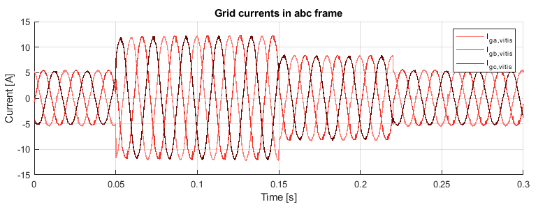
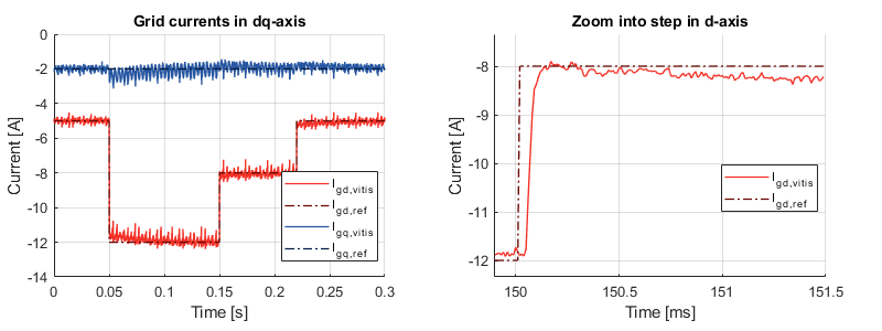
Various reference steps are performed on the d- and q-axis current references to validate the reference tracking and perturbation rejection abilities of the developed algorithm.
The graph below shows the measured grid currents when the d-axis current reference takes the values 5, 12, and 8 A.
When projected into the dq rotating reference frame, the measured grid currents give the following results. It can be seen that the current reference is successfully and rapidly tracked by the d-axis controllers and that the perturbation is well rejected on the q axis.
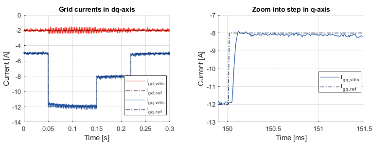
If the same reference steps are performed on the q-axis, the same observations can be made.
Creation of the Vivado block design
This section provides a step-by-step explanation of how to re-create the Vivado project to generate the FPGA bitstream of the Grid-tied inverter control.
To find all FPGA-related notes, you can visit the FPGA development homepage.
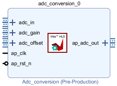
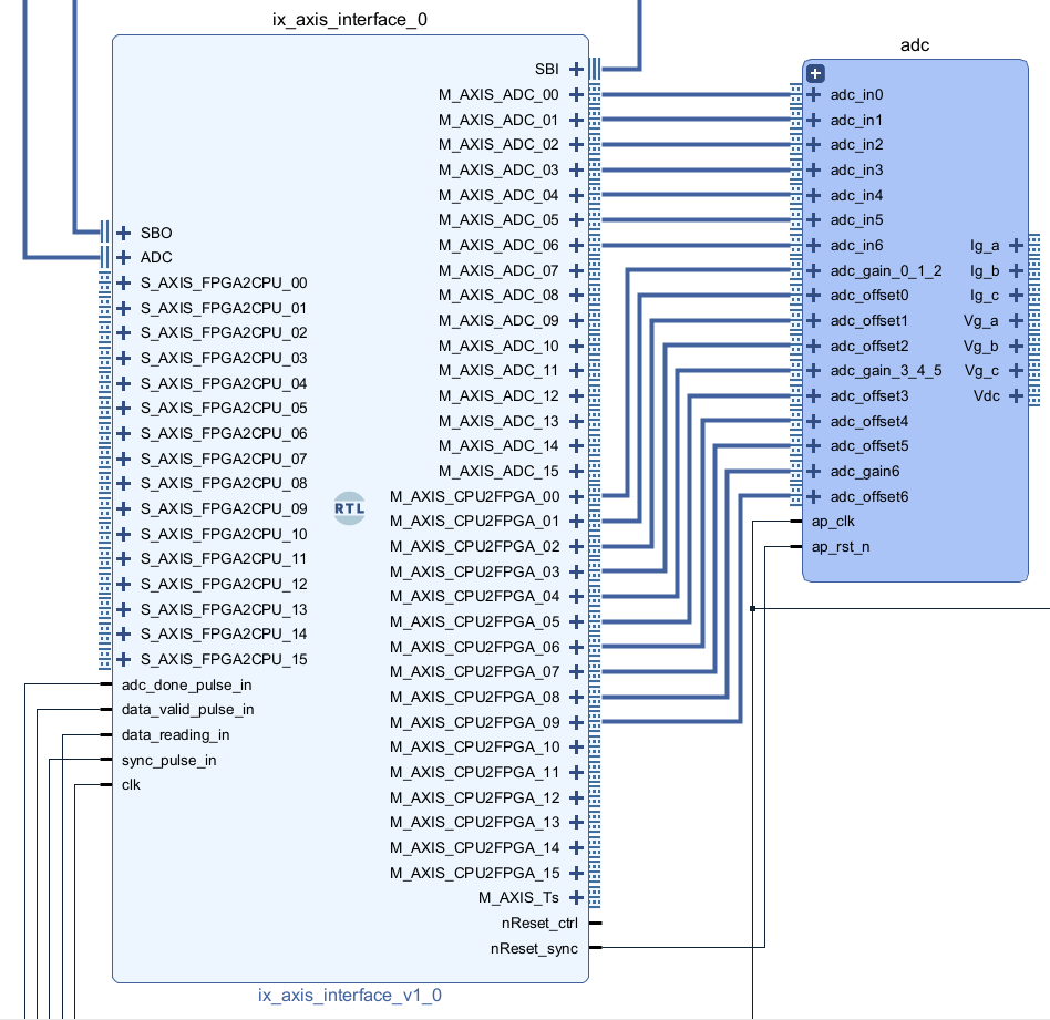
Raw ADC data conversion
The ADC conversion results are available from the AXI4-Stream interfaces M_AXIS_ADC of the “ix axis interface” module. They return the raw 16-bit signed integer result from the ADC chips.
The ADC conversion IP shown below serves to convert that raw data into the actual measured quantities in the float datatype. Knowing the sensitivity \(S\) of the sensor and the B-Box RCP front-end gain \(G\), the formula below can be used:
\(\alpha [\text{bit/A}] = S\cdot G\cdot 32768/10\,\)

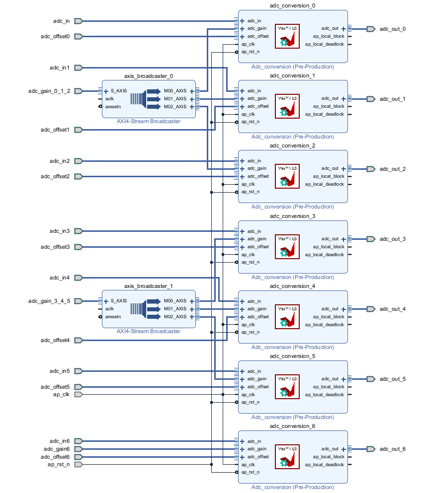
This ADC conversion module is connected as shown in the two screenshots below. The AXI4-Stream Broadcaster IP (included with Vivado) serves to propagate an AXI4-Stream to multiple ports.
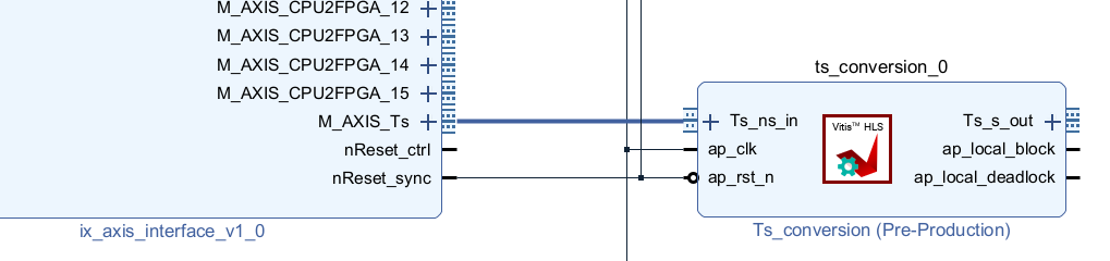
Sample time (Ts) conversion
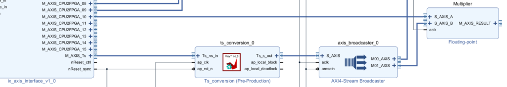
The M_AXIS_Ts port of the “ix axis interface” provides the sample period \(T_s\) in nanoseconds in a 32-bit unsigned integer format. This signal is the time distance between two consecutive samples.
The Ts conversion module shown below converts this signal into a floating-point value in seconds. The result will be used by the PI controllers of the Grid synchronization module and the dq current control module.
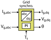
Grid synchronization
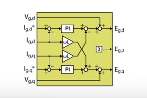
The grid synchronization is done using the dq-type PLL which transforms both the grid voltages and currents into dq components, that are used in the dq current controller.
The grid synchronization IP shown below is documented in the FPGA impl. of a PLL for grid sync page.
In the Vivado project, the IP is connected as follows. An AXI4-Stream Broadcaster is used because the sample time (Ts) signal is also connected to the dq current controller as shown in the next section.
DQ current control
The implementation of the dq current controller is detailed in FPGA-based PI for dq current control. It consists of two identical PI controllers with a decoupling network for independent control of the d- and q-components of the grid current.
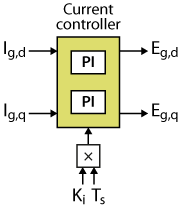
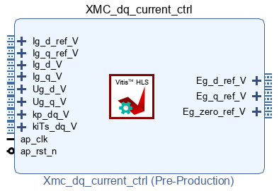
The kiTs_dq port takes as input the results of Ts multiplied by Ki (Ki is a parameter set from the CPU, using the port CPU2FPGA_10). The multiplication is performed using a Floating-Point IP as shown below.
The dq current controller is connected as shown below. The inputs Kp, Id_ref, and Iq_ref are connected to CPU2FPGA ports 11, 12, and 13.
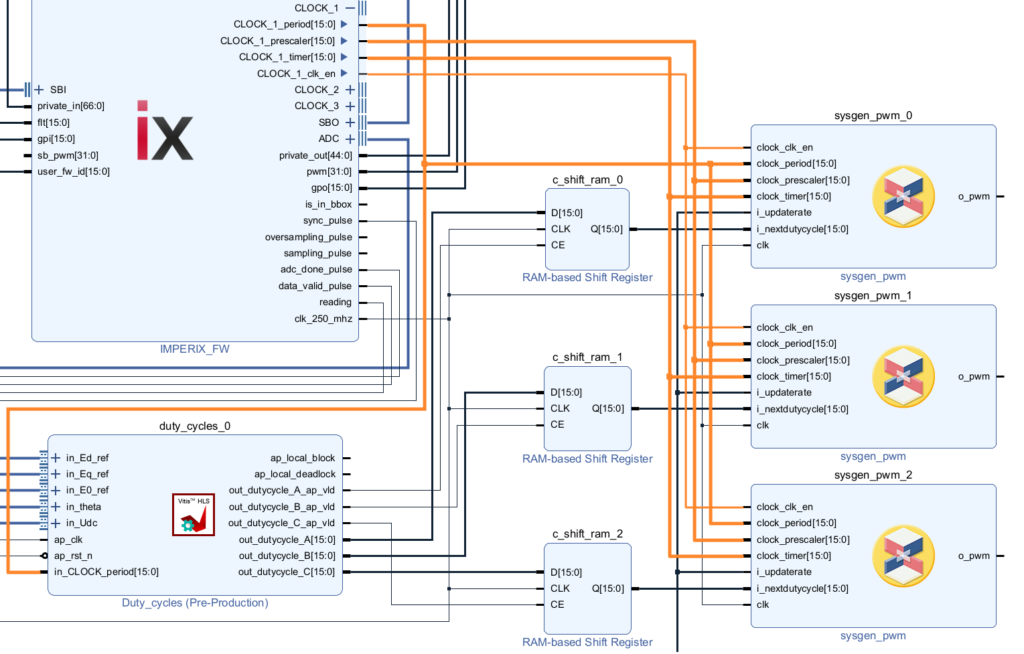
Duty cycles computation
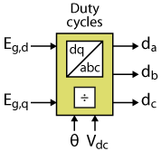
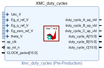
This block converts the voltage references computed by the dq current controller to abc quantities \(E_{g,abc}\), and computes the corresponding duty cycles (in the range [0,1]) according to
$$ d_{abc} = \left(\frac{E_{g,abc}}{V_{dc}}+0.5\right)\cdot T_\text{clk},$$
where \(T_\text{clk}\) is the period of the clock used in the PWM modulator, expressed in ticks (1 tick = 4 ns). The duty cycles are converted into uint16 numbers with a unit of ticks to be compatible with the PWM modulator.
It is connected as shown below. in_CLOCK_period is connected to CLOCK_1_period of the IMPERIX_FW IP.
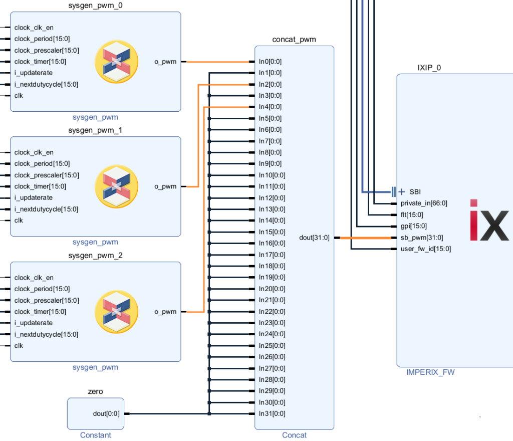
PWM generation
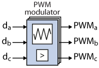
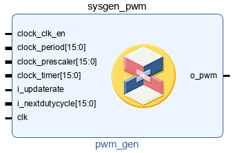
Finally, the duty cycles are transformed into PWM signals in the PWM modulator block. The implementation details are presented in PWM modulator implementation in FPGA.
The PWM block uses the clock signal CLOCK_1 as a reference to generate the PWM triangular carrier signal. The switching frequency is therefore equal to the frequency of CLOCK_1, which can be configured using a CLK block.
The high-side switching signals are obtained by comparing the 3 duty cycles \(d_{abc}\) with the triangular carrier. The generation of the low-side switching signals is done by the SB-PWM driver incorporated into the imperix IP and the dead time duration is specified in the CPU block Sandbox PWM configurator.
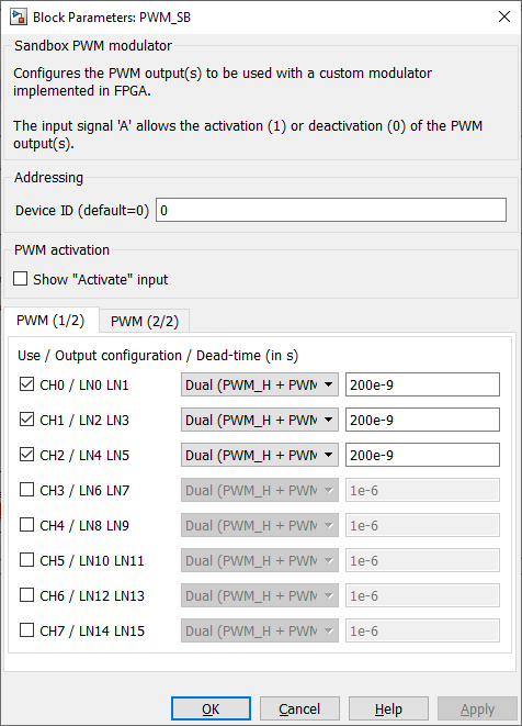
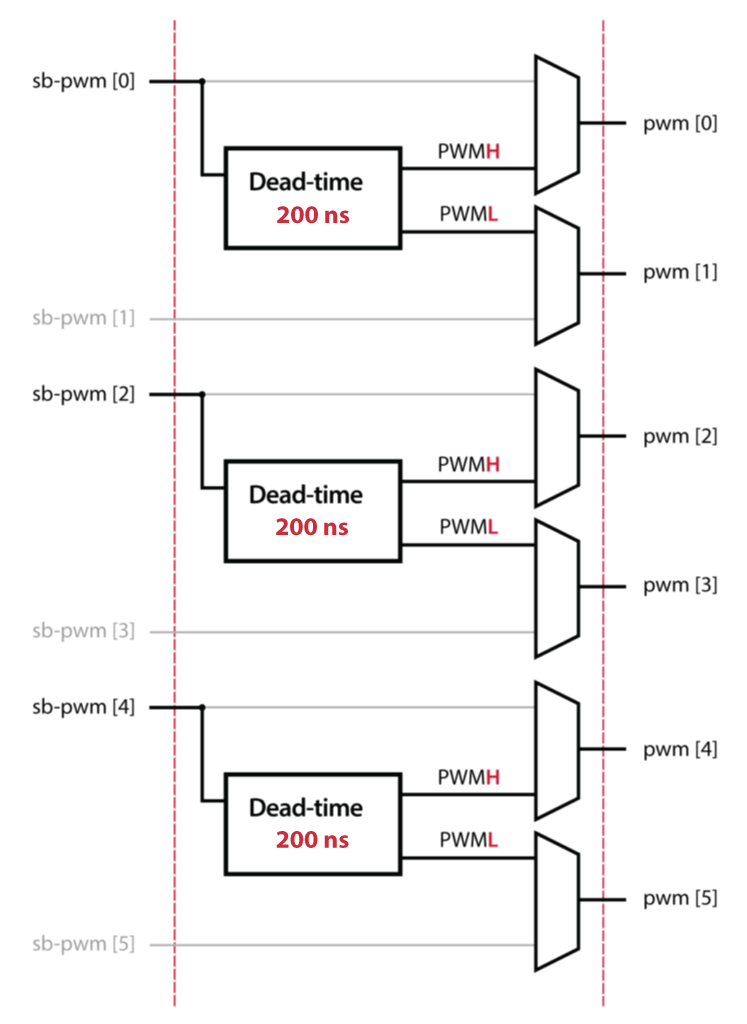
Thanks to the SB-PWM driver, the safety mechanism of the B-Box RCP is also available for custom-made PWM modulators. In case an over-value is detected during operation, the PWM outputs are immediately blocked and the operation is safely stopped.
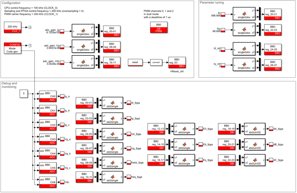
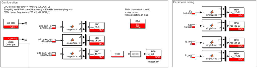
CPU-side implementation
The CPU model shown below is only used for the following tasks:
Configuration:
- Configure the sampling frequency using the Configuration block (CLOCK_0 = 100 kHz, oversampling = 4)
- Configure the modulator clocks using the CLK block (CLOCK_1 = 200 kHz)
- Configure the ADC conversion parameters (gain and offset)
Parameter tuning:
- Tune the controller gains (Kp and Ki)
- Transfer the dq current references \(I_{g,d}^*\) and \(I_{g,q}^*\) to the FPGA
Debugging and monitoring
For debugging and monitoring purposes, internal signals of the FPGA inverter control model can be split using AXI4-Stream Broadcaster IPs and routed to FPGA2CPU ports of the imperix IP. This way, the signals can be accessed from the CPU, connected to probe variable blocks, and observed using Cockpit.
Additionally, ADC blocks can still be used to observe the analog input signals. For accurate readings, make sure the sensitivities of the ADC blocks match the gain parameter sent to the FPGA!