
Table of Contents
The CONFIG block primarily configures the main clock (CLK0) and its derivatives. Together, these clocks define the frequency and phase of the sampling events, as well as the CPU interrupt (which triggers the execution of the control task). CLK0 is indispensable to the proper operation of the hardware, as is the CONFIG block.
Secondary configuration options are also appended to the CONFIG block, such as:
- The model execution purpose (Simulink only) – See PN134.
- The target hardware generation (Simulink only) – See PN134.
- Solver parameters – See below.
- Plant-side modeling options – See PN150.
The CONFIG block is available on all imperix controllers and behaves identically across them.
Key principles of operation
Imperix controllers have a specialized timing architecture that minimizes latency and supports networked control, as described in PN253. In total, four configurable clocks are available:
- CLK0 deserves particular attention as it is always active and is statically associated with the sampling and control tasks. CLK0 is also limited to a constant frequency, thereby imposing regular sampling.
- CLK1-CLK3 are optional signals that can have variable frequencies. These clocks can be freely associated with different modulators (see CLK block).
Several clocks are derived from CLK0, the two most important of which are:
- The sampling clock SCLK, of frequency FSCLK. It only differs from CLK0 by a configurable phase shift.
- The CPU interrupt, responsible for launching the control task, of frequency FCPU. If needed, FCPU can be defined as a decimated derivative of FSCLK using a post-scaling coefficient.
More information about the related resources is given in PN253. Further details on the general operating principles of imperix controllers are provided in PN261.
Typical timing configurations
When working with the ACG SDK, the timing configuration for sampling, control, and modulation is determined by wiring the corresponding blocks to the four time bases (i.e., CLK0-CLK3). The most common configurations are described in detail in PN259 and summarized below:
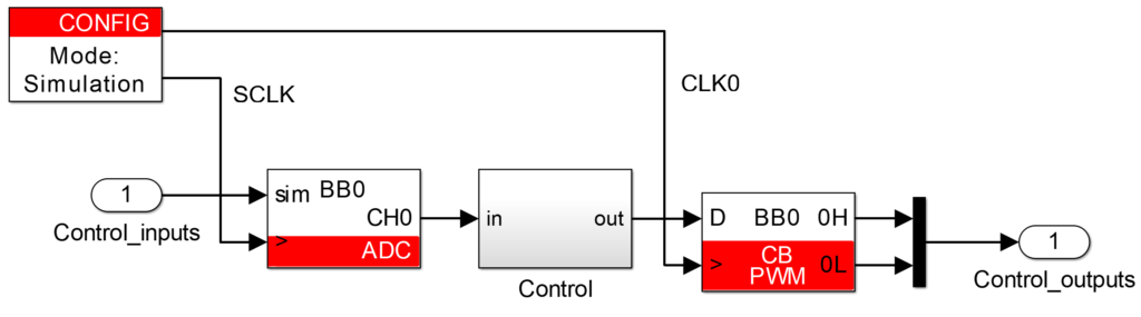
- Single-rate sampling, in which case the control task is executed once per PWM period. Sampling, control, and modulation are all linked to CLK0, with adequate phase shifts. This case is the default configuration implemented in most examples and illustrated below:
- Double-rate sampling, in which case the control task is executed twice per PWM period. Sampling and control are linked to CLK0 (with adequate phase shift), whereas modulation must be linked to another clock (e.g., CLK1), configured at half the frequency of CLK0. This case gives best performance, provided that sufficient CPU time is available. Read more in PN259.
- Advanced sampling configurations are also possible, typically authorizing the retrieval of multiple samples at once (data history), variable-frequency switching, or running FPGA-based control tasks at a higher rate than the CPU. Read more in PN259.
In Simulink/PLECS, the two clocks available as outputs of the CONFIG block can be easily used to implement the scenarios described above. In practice, they serve the following two purposes:
- In simulation mode, the sampling clock SCLK is indispensable for accurately modeling the sampling instant and the discrete nature of the control’s execution. Similarly, CLK0 is important for determining the relative phase of the modulation with respect to sampling, as well as phase shifts between modulators.
- In code generation mode, these signals do not generate any software variables but are analyzed by Simulink/PLECS to map the connected resources to the physical hardware clocks.
More details regarding how Simulink and PLECS handle these aspects are presented in PN135 (Simulink) and PN137 (PLECS).
Block parameters
Timings
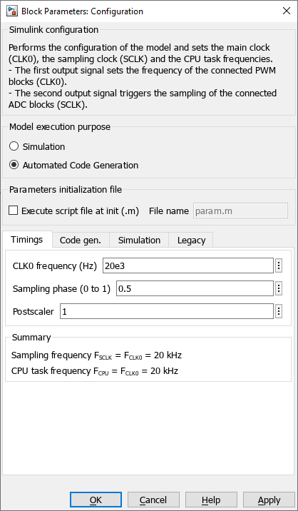
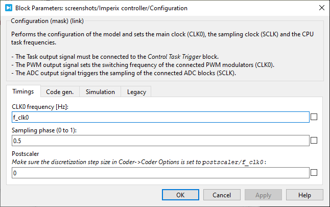
- The CLK0 frequency sets the main clock frequency FCLK0, which provides the time base for generating the ADC sampling strobe SCLK.
- The sampling phase sets the phase shift of the ADC sampling strobe SCLK relative to CLK0. The CPU control task is executed immediately once the values are available. If the modulators are also tied to CLK0, there are equivalences between phase-shifting the sampling and the modulation.
- The postscaler is used to decimate the CPU task execution rate relative to SCLK such that
FCPU = FCLK0 /postscaler.
Code generation
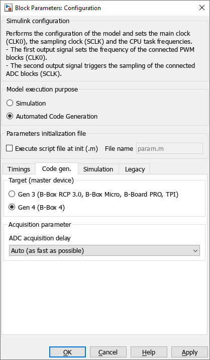
- The Target is a Simulink-specific parameter that defines which hardware the code will be generated for. In PLECS, the equivalent parameter is located in Coder -> Coder option… (Ctrl+Alt+B). The two possible options are:
- Gen 3 (B-Box RCP3.0, B-Box Micro, B-Board PRO, TPI)
- Gen 4 (B-Box 4 only)
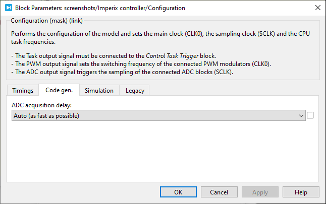
- The ADC acquisition delay corresponds to the complete conversion time, measured from the ADC sampling instant (identical for all channels) to the time the data becomes available in the CPU cache, just before the execution of the control task. This parameter can take multiple values among imperix controllers. The available options are:
- Auto (as fast as possible, recommended) – This automatically selects the fastest option. This is identified at launch time, as slaves may be connected to the target.
- 2 μs (all devices) – This conservative legacy setting is available for all controllers.
- 500 ns (all devices except B-Box RCP 3.0) – This setting is available for all controllers except B-Box 3.
- 200/368 ns (B-Box 4 only) – This high-performance setting is only available on B-Box 4.
Simulation
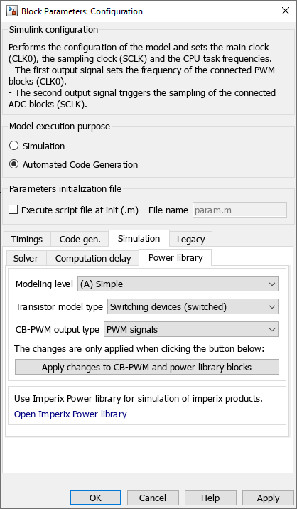
- Basic Solver parameters can be directly set in the associated tab. These come from the “Model Configuration Parameters” (Ctrl+E), which are automatically synchronized with them. These solver parameters only apply to the variable-step solver used in simulation mode.
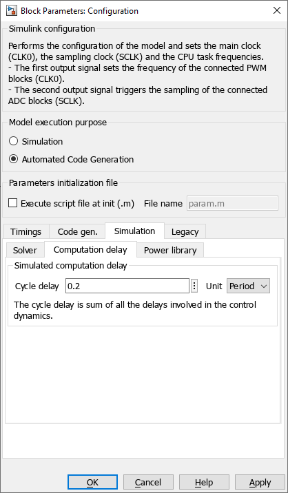
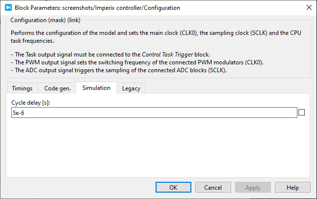
- The Computation delay is exclusively used in simulation mode. It accurately models the total time required to compute the control task, thereby affecting the moment at which the PWM parameters are actually updated. As such, it summarizes the delays in the control dynamics (ADC acquisition, data read, control task execution, data write).
- The Power library parameters are documented in PN150.
Legacy parameters
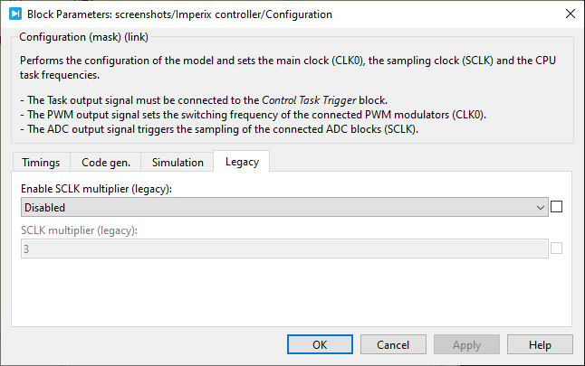
- The SCLK multiplier parameter allows setting a multiplier such that FSCLK = FCLK0 x
multiplier. This parameter is maintained for legacy reasons. To obtain a sampling frequency higher than the CPU execution frequency, it is recommended to increase FCLK0 and use the postscaler instead.
Simulink block
Signal specification
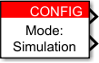
The behavior of these signals during simulation is described in PN135.
Mask
PLECS block
- The
Taskoutput must be connected to the Control Task Trigger block. The Control Task Triggernominal base sample timemust be equal topostscaler/CLOCK_0frequency. - The
PWMclock signal must be connected to the>input of the PWM blocks to set their frequency to the CLK0 frequency. - The
ADCclock output is the sampling signal SCLK. It must be connected to the>input signal of all the ADC blocks.

The behavior of these signals during simulations is described in PN137.
Mask
Changing the postscaler in PLECS
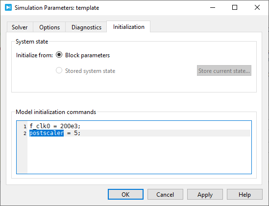
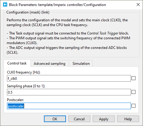
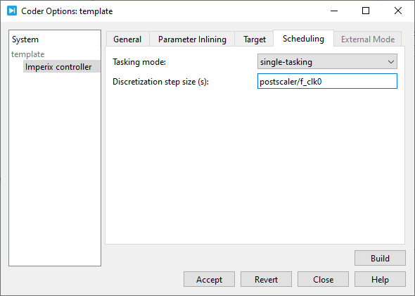
In PLECS, the discretization step size must match the CPU control task period for the generated code to behave properly. When using the postscaler, the discretization step size must be set to postscaler/FCLK0. A simulation variable can be used for convenience, as illustrated below:
1. Create a postscaler variable in Simulation -> Simulation parameters (Ctrl+E).
2. Use the postscaler variable in the CONFIG block mask.
3. Update the discretization step size in Coder -> Coder options (Ctrl+Alt+B)
 By Benoît Steinmann • April 2, 2021 • SD002
 By Stéphane Lovejoy • March 21, 2021 • PN137
 By Julien Orsinger • March 23, 2021 • PN135