Table of Contents
The PEH block is a simulation model included in the Imperix Power library. It models the imperix full-bridge module PEH4010 and PEH2015 in Simulink and PLECS simulation.
For more information regarding the Imperix Power library, please read Getting started with Imperix Power library.
• ACG SDK 2024.2: First release. Support for PLECS and Simulink SPS library (“Black” blocks).
• ACG SDK 2025.2: Addition of thermal models for most PEB and PEN modules.
• ACG SDK 2026.1: Support for the latest products (PEB-800-40, VSR-1000-ISO, VSR-500-HBW, CSR-25-HBW).
• ACG SDK 2026.1.3: Support for Simulink Simscape Electrical library (“Blue” blocks).
• Simulink (R2016a or newer): Simscape is required.
• Plexim PLECS (4.5 or newer): No particular requirement.
Additionally, for Simulink:
• Simscape Electrical library: Simscape Electrical is required.
• SPS library: Simscape Specialized Power Systems (up to R2025b) or OPAL-RT SPS Software is required.
Modeling of PEH
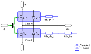
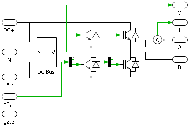
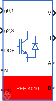
The schematic of the PEH model is depicted on the right. It has two modeling levels:
- (A) Simple
- (B) Detailed
For more detailed model parameters and measurement results, please contact [email protected].
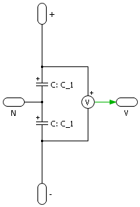
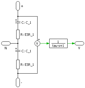
DC bus
The schematic of the equivalent DC bus is shown below.
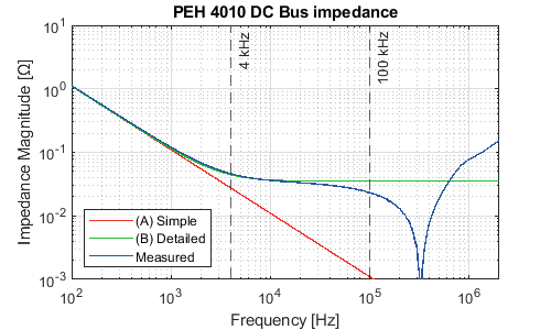
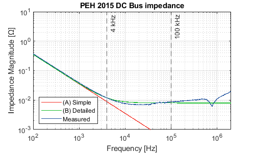
The simulation model is relevant within a given frequency range. The frequency validity range is 0-4 kHz for the (A) Simple level and 0-100 kHz for the (B) Detailed level. In that range, the impedance and transfer function of the model are reasonably close to the modeled system, which can be seen along with the plots of the proposed models. The model parameters are also displayed below.
| C_1 [uF] | ESR_1 [mΩ] | |
| (A) | 1450*2 | 0 |
| (B) | 1450*2 | 35/2 |
| C_1 [uF] | ESR_1 [mΩ] | |
| (A) | 4500*2 | 0 |
| (B) | 4500*2 | 8/2 |
Embedded sensors
A generic sensor can be approximately modeled by an ideal sensor in series with an optional first-order Low-Pass Filter (LPF). The relationship between sensor’s bandwidth \(f_{BW}\) and the time constant \(\tau\) of the LPF follows \(\tau = \frac{1}{2\pi f_{BW}}\).
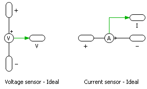
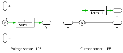
A sensor is modeled as a first-order LPF only if its bandwidth lies within the frequency range of a given modeling level. Otherwise, it is modeled as an ideal sensor. The following table summarizes the information on all the sensors in the PEH.
| Sensor | Bandwidth [kHz] | (A) Simple | (B) Detailed |
|---|---|---|---|
| PEH voltage sensor | 25 | Ideal | LPF |
| PEH current sensor | 120 | Ideal | Ideal |
Power transistors
The PEH block offers two options for modeling the power transistors:
- Switched The transistors are modeled by individual power semiconductors. The control inputs are instantaneous logical gate signals.
- Averaged The transistors are modeled by controlled voltage and current sources. The control inputs are the relative on-times of the semiconductors with values between 0 and 1. The gate signals can be either instantaneous (using only values 0 and 1) or time-averaged.
Although the functionality is practically the same, these options are named differently in PLECS and Simulink Simscape to be consistent with their naming conventions.
In Simulink Simscape they are named:
- Switching devices
- Switching function
In PLECS they are named:
- Switched
- Sub-cycle average
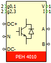
Simulink PEH block
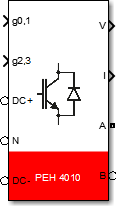
Port specification
- The input
g0,1andg2,3are the gate signals. There are 4 signals in total, and the order is shown in the schematic.- For
Switching devices (switched)model,g0,1andg2,3are the 0/1 PWM signals. - For
Switching Function (averaged)model,g0,1andg2,3can be either the 0/1 PWM signals or the duty cycles between 0 and 1.
- For
- The output
Vis the measured voltage across the DC bus. - The output
Iis the measured output current. - The connection port
DC+is the electrical port connected to the positive pole of the DC bus. - The connection port
DC-is the electrical port connected to the negative pole of the DC bus. - The connection port
Nis the electrical port connected to the midpoint of the DC bus. - The connection port
AandBare the electrical ports connected to the AC output.
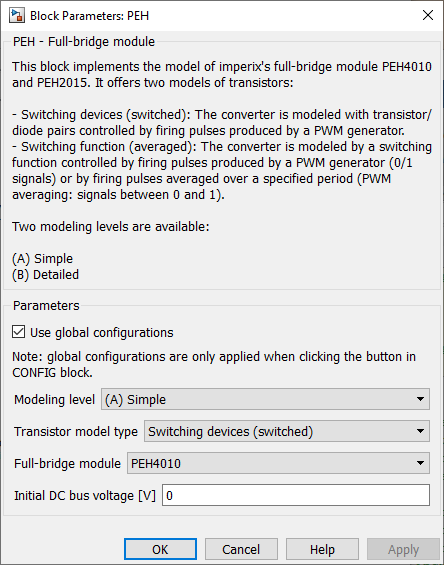
Parameters
Use global configurationsis ticked when the block receives global configurations from theConfigblock.Modeling levelselects the modeling level of the peripheral circuits.Transistor model typeselects the model of the power transistors.Full-bridge moduleselects the type of PEH products to be simulated.Initial DC voltage [V]defines the initial voltage across the DC bus when the simulation starts.
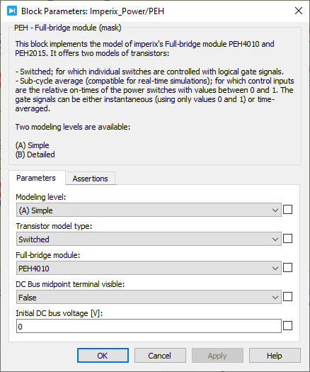
PLECS PEH block
Port specification
- The input
g0,1andg2,3are the gate signals. There are 4 signals in total, and the order is shown in the schematic.- For
Switchedmodel,g0,1andg2,3are the 0/1 PWM signals. - For
Sub-cycle averagemodel,g0,1andg2,3can be either the 0/1 PWM signals or the duty cycles between 0 and 1.
- For
- The output
Vis the measured voltage across the DC bus. - The output
Iis the measured output current. - The connection port
DC+is the electrical port connected to the positive pole of the DC bus. - The connection port
DC-is the electrical port connected to the negative pole of the DC bus. - The connection port
Nis the electrical port connected to the midpoint of the DC bus. - The connection port
AandBare the electrical ports connected to the AC output.
Parameters
Modeling levelselects the modeling level of the peripheral circuits.Transistor model typeselects the model of the power transistors.Full-bridge moduleselects the type of PEH products to be simulated.DC Bus midpoint terminal visibleshows or hides the portN.Initial DC voltage [V]defines the initial voltage across the DC bus when the simulation starts.
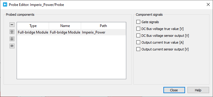
Probe signals
The following signals can be monitored by a Probe block in PLECS.
Gate signalsmonitors the gate signals present at the inputg0,1andg2,3.DC Bus voltage true value [V]monitors the true value of the DC bus voltage in Volt.DC Bus voltage sensor output [V]monitors the physical output of the DC bus voltage sensor in Volt.Output current true value [A]monitors the true value of the output current in Amp.Output current sensor output [V]monitors the physical output of the output current sensor in Volt.