Table of Contents
Dead time is a brief non-conduction interval imposed across two complementary PWM signals to prevent a potentially damaging shoot-through inside the corresponding switching cell. Dead time insertion is therefore a critical mechanism for the safety, reliability, and efficiency of most power converter topologies.
The dead time duration must be long enough to accommodate variations of the switching dynamics (influenced by DC link voltage, current, and temperature), yet short enough to avoid unnecessary distorsion of the output current distortion as well as excessive losses. This article details the calculation of the minimum and recommended dead time values for imperix controllers and power modules.
Design procedure for dead time selection
Inspired from [1], the proposed design procedure mainly depends on two factors:
- Propagation delay asymmetries along the PWM signal transmission chain
- Semiconductor delay asymmetries between turn-on and turn-off events
Complementary PWM signals frequently exhibit propagation delay asymmetry, which is attributable to component variability along the signal chain or disparate signal paths. The figure below illustrates the components involved along a typical transmission chain with a B-Box controller and a power module. The total propagation delay asymmetry can be subdivided into three distinct components:
- \(T_1\) : the propagation delay asymmetry due to the controller;
- \(T_2\) : the propagation delay asymmetry due to the mezzanine board;
- \(T_3\) : the propagation delay asymmetry due to the gate drivers (incl. protection logic);
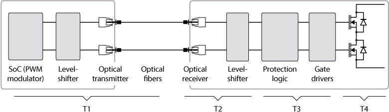
The preceding figure also introduces \(T_4\), the turn-on/turn-off time asymmetry inherent to the power semiconductors. Non-instantaneous switching in MOSFET and IGBT devices, attributed to intrinsic parasitic capacitances [2], indeed necessitates the consideration of four distinct delays:
- \(T_{d,off}\) : the turn-off time;
- \(T_{f}\) : the fall time;
- \(T_{d,on}\) : the turn-on time;
- \(T_{r}\) : the rise time.

Since the total turn-off duration is typically longer than the turn-on one [1], it results in an asymmetry, which is computed as follows:
$$ T_4 = (T_{d,\text{off}} + T_{f}) – (T_{d,\text{on}} + T_{r}) $$
Considering both switching and propagation delay asymmetries is crucial to prevent the simultaneous conduction of two power semiconductors within the same phase-leg. The minimum dead time, as proposed in [1], can therefore be calculated using the following formula:
$$ DT_{minimum} = (T_1 + T_2 + T_3 + T_4)\cdot 1.2 $$
where the 1.2 factor corresponds to a 20% safety margin.
Dependency on operating conditions
The turn-on/turn-off time asymmetry is highly dependent on operating conditions, including the DC link voltage, load current, and temperature, making the minimum dead time a dynamic parameter. Implementing the shortest possible dead time is often desirable to reduce conduction losses in the anti-parallel diode and minimize output voltage distortion. While real-time dead time adjustment is feasible [3], it introduces additional complexity. Therefore, this article employs a constant dead time.
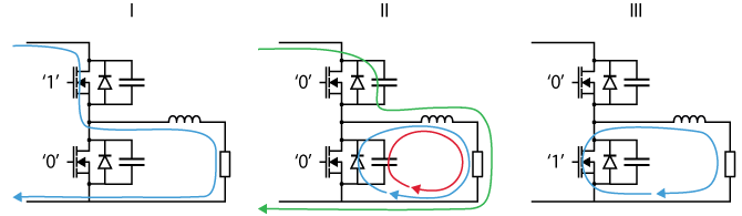
To avoid shoot-through, the constant dead time should be chosen under the worst operating conditions. The rise and fall times are constrained by the parasitic output capacitance (\(C_{oss}\)) [2]. Consequently, efficient \(C_{oss}\) charging and discharging is critical for dead time minimization. The following case study, based on a buck converter, illustrates the influence of the load conditions [4].
- Zone I: the upper switch conducts, while the bottom switch blocks the DC bus voltage. For this reason, the parasitic output capacitance \(C_{oss}\) of the bottom switch is fully charged.
- Zone II: during the dead time, the bottom \(C_{oss}\) discharges itself in the load through the red path. The higher the load current, the faster the discharge. Similarly, the upper \(C_{oss}\) charges itself through the green path.
- Zone III: the bottom switch is turned on. At this moment, the upper \(C_{oss}\) is fully charged.
The smaller the load current, the longer it takes for the upper switch to turn off, thus increasing the minimum required dead time. For this reason, the dead time should be computed under light load conditions.
Timing information
T1 – Control platform (PWM signal source)
The digital controllers developed by imperix generate PWM signals utilizing an integrated FPGA. These signals are subsequently level-shifted to attain output voltages of either 3.3V or 5V. Following this, the signals are converted into optical outputs via an integrated optical transceiver, enabling transmission through fiber optic cables to the power modules. A summary of the maximum propagation delay asymmetry between paired PWM output lanes is provided in the following table.
| Control system | T1[ns] |
|---|---|
| BoomBox 2 (on optical PWM outputs) | 36 |
| B-Box RCP 3.0 (on optical PWM outputs) | 13 |
| B-Box RCP 3.0 (on electrical PWM outputs) | 2.3 |
| B-Box Micro (on optical PWM outputs) | 13 |
| B-Box 4 (on optical PWM outputs) | 9.3 |
| B-Box 4 (on electrical PWM outputs) | 3.3 |
| B-Board PRO (electrical PWM outputs) | 2.5 |
| TPI8032 | 2.5 |
T2 – Mezzanine boards of imperix power modules (optical receivers)
Mezzanine boards are compact printed circuit boards (PCBs) designed for integration atop imperix power modules. These boards incorporate optical receivers for pulse-width modulation (PWM) input signals and a level shifter to ensure voltage compatibility with the power module’s on-board logic. The cumulative propagation delay asymmetry attributed to these components is detailed below:
| Power module | T2[ns] |
|---|---|
| PEB-800-40 | 9.5 |
| PEB8024*, PEB8038, and PEB4050 | 13 |
| PEN8018* | 13 |
| PEH2015 and PEH4010 | 25 |
| TPI8032 (no mezzanine) | 0 |
| PEB8032 and PEB4046 (discontinued) | 20 |
* Units sold in 2019 or before have a longer delay of 25 ns, rather than 13 ns.
T3 – Power modules (protection logic and gate drivers)
Gating signals undergo initial processing by a Complex Programmable Logic Device (CPLD) or a Field-Programmable Gate Array (FPGA). A key function of this component is to inhibit PWM signals upon the detection of a fault condition. Following this, the PWM signals are further processed by gate drivers, which introduces an additional propagation asymmetry. The table presented below summarizes the total propagation delay asymmetry, categorized by module type:
| Power module | T3[ns] |
|---|---|
| PEB-800-40 | 22 |
| PEB8024, PEB8038, and PEB4050 | 32 |
| PEN8018 | 52 |
| PEH2015* and PEH4010* | 52 |
| TPI8032 | 32 |
| PEB8032 and PEB4046 (discontinued) | 155 |
* Units sold before 2018 (revision 5 or older) had a larger potential assymetry of 500 ns, rather than 52 ns.
T4 – Power semiconductors
The following table present typical timings for the power semiconductors at selected operating points:
| Power module | Operating conditions | Td,off | Tf | Td,on | Tr | T4[ns] |
|---|---|---|---|---|---|---|
| PEB-800-40 | 800V, 6A | 39 | 105 | 48 | 41 | 55 |
| PEB8024 | 760V, 10A | 35 | 18 | 16 | 17 | 20 |
| PEB8038 | 760V, 5A | 287 | 133 | 68 | 82 | 270 |
| PEB4050 | 400V, 2.5A | 116 | 100 | 101 | 15 | 100 |
| PEN8018 | 760V, 5A | 210 | 202 | 32 | 40 | 340 |
| PEH2015 | 200V, 2A | 102 | 112 | 26 | 78 | 110 |
| PEH4010 | 400V, 2A | 115 | 147 | 24 | 88 | 150 |
| TPI8032 | 800V, 5A | 95 | 60 | 42 | 26 | 87 |
| PEB8032 (discontinued) | 700V, 32A | – | – | – | – | 380 |
| PEB4046 (discontinued) | 400V, 46A | – | – | – | – | 550 |
Dead time computation example
The proposed example is a B-Box 4 controlling a boost-type DC/DC converter made of one PEB-800-40. Following the above-presented design procedure, the minimum dead time is:
$$ DT_{min} = (T_1 + T_2 + T_3 + T_4) \cdot 1.2= (9.3 + 9.5 + 22 + 55) \cdot 1.2 = 115 \,\text{ns} $$
The following table summarizes the minimum and recommended dead times for typical configurations.
| Control system | Power module | Minimum dead time [ns] |
|---|---|---|
| B-Box 4 | PEB-800-40 | 115 |
| B-Box RCP3.0 | PEB8024 | 100 |
| B-Box RCP3.0 | PEB8038 | 400 |
| B-Box RCP3.0 | PEB4050 | 200 |
| B-Box 4 | PEN8018 | 495 |
| B-Box 4 | PEH2015 | 235 |
| B-Box 4 | PEH4010 | 285 |
| TPI8032 | TPI8032 | 124 |
Going further with dead time selection
Dependence of dead time on operating conditions
The design procedure reveals that power semiconductor switching dynamics are the principal criteria for dead time selection. Specifically, \(T_{d,off}\) is the most influential timing parameter, and is also highly sensitive to operating conditions and effective collector/drain impedance. The key observations include:
- SiC MOSFET Sensitivity: Due to low parasitic output capacitance, SiC MOSFETs exhibit high sensitivity to load impedance, which can significantly increase the complete turn-off time (e.g., a fivefold increase is reported in [5]), challenging the assumption of an ideal inductive load.
- Low Current Dynamics: The switching trajectory may vary considerably at very small drain currents [3]. However, the prolonged drain voltage rise time in these conditions does not typically require an extension of the dead time for shoot-through prevention, as current-related dynamics are faster.
- Procedure vs. Optimization: While the proposed procedure mandates a full turn-off before the complementary switch turns on, allowing a limited circulating current at light load can accelerate the switching process. This optimization, however, is not easily implemented in a standard configuration.
Dead time compensation techniques
The introduction of dead time unavoidably impacts the average output voltage. Depending on the current direction, the resulting voltage may deviate from the desired value [6]. This effect is most pronounced when the dead time is long with respect to the switching period.
The predictable impact on average voltage can be compensated for in software. Current feedforward dead time compensation [6] provides an example, as utilized in TN111.
Dynamic dead time optimization
As the system efficiency is often negatively impacted by dead time, it may be worth optimizing the dead time during run-time, as a function of the operating conditions. For instance, the authors of [3] report that the overall power losses can be reduced by up to 18% using such a technique.
Pragmatically, some improvements are also certainly already achievable using a dead-time that is “only” a function of the load current (which is often an already-available measurement). This could typically be implemented using a look-up table.
References
[1] Infineon, “Application Note AN2007-04: How to calculate and minimize the dead time requirement for IGBTs properly”, on Infineon’s website, May 2007.
[2] J. Lutz, H. Schlangenotto, U. Scheuermann and R. De Doncker, “Semiconductor Power Devices – Physics, Characteristics, Reliability,” Springer, 2011. (e-ISBN 978-3-642-11125-9)
[3] Z. Zhang, H. Lu, D. J. Costinett, F. Wang, L. M. Tolbert and B. J. Blalock, “Model-Based Dead Time Optimization for Voltage-Source Converters Utilizing Silicon Carbide Semiconductors,” in IEEE Trans. on Power Elect., Nov. 2017.
[4] Texas Instruments, “Application Report SLVA504A: Calculating Power Dissipation for a H-Bridge or Half Bridge Driver”, on TI’s website, February 2012, Revised July 2021
[5] Z. Zhang, F. Wang, L. M. Tolbert, B. J. Blalock and D. J. Costinett, “Evaluation of Switching Performance of SiC Devices in PWM Inverter-Fed Induction Motor Drives,” in IEEE Trans. on Power Elect., Oct. 2015.
[6] F. Blaabjerg, J. K. Pedersen and P. Thoegersen, “Improved modulation techniques for PWM-VSI drives,” in IEEE Transactions on Industrial Electronics, vol. 44, no. 1, pp. 87-95, Feb. 1997