Table of Contents
As introduced in PN118, SFP communication constitutes a convenient way to interconnect devices. Widely used, it offers an efficient layer on which protocols such as Aurora can be implemented to exchange data.
In this example, the SFP communication connects a B-Box RCP (or B-Board PRO) to a HIL simulator from RTDS. It makes the bridge between the control – executed in the B-Box RCP (or B-Board PRO) – and a simulation model of an MMC converter running on the GTSOC board.
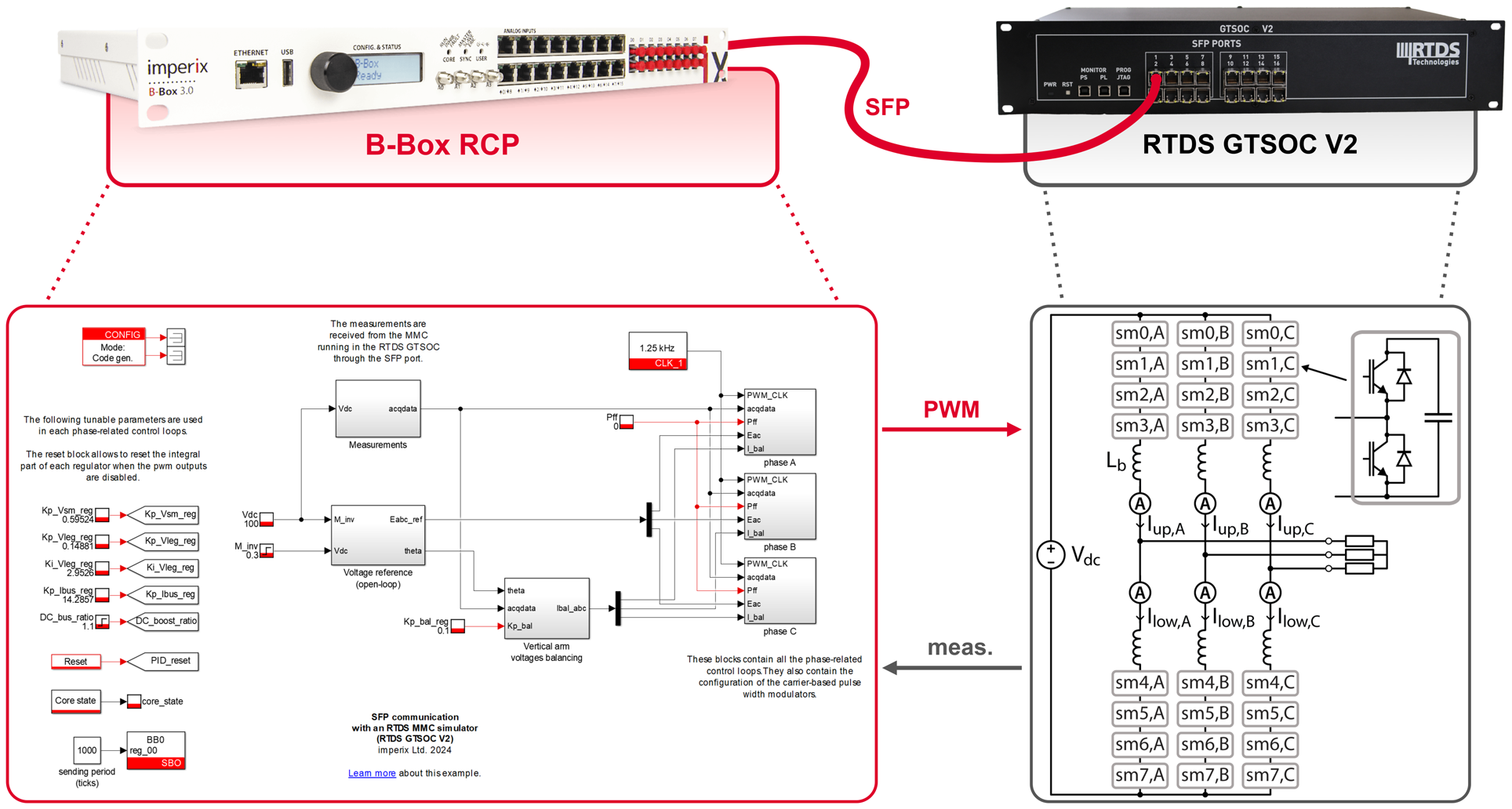
Following the configuration of the MMC bundle, the simulated MMC contains 6 arms and 4 submodules per arm, as shown in Fig. 1. The closed-loop model provided to show proper communication and control of the MMC is also directly adapted from the AN009.
Communication chain
The control and communication chain is depicted in Fig. 2. The closed-loop control running in the CPU of the B-Box controller generates duty cycles, which are converted to PWM signals by the carrier-based modulator (CB-PWM). These PWM signals are directly available in the FPGA, where they are packed into frames by the RTDS MMC driver and transferred to the MMC simulation model via Aurora 8B/10B.
The simulation model outputs computed voltages and currents, as well as additional real-time data (e.g. submodules status), and sends them back as Aurora frames to the B-Box (or B-Board). Once received, the frames are decoded by the driver and their content is made available to the B-Box CPU through SBI registers.
Required software
- Xilinx Vivado 2022.1 or later (previous versions may work but have not been tested).
Installation guide available here. - FPGA sandbox template 3.10 or later.
Available on the FPGA download page. - C++ or ACG SDK version 2024.3 or later.
Available on the SDK download page.
Downloads
The Simulink model running in the CPU and the Vivado project to generate the FPGA bitstream are available below.
Simulink model
Vivado project generation scripts
Results
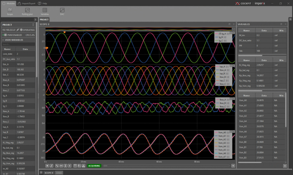
As shown in Fig. 3, the closed-loop control generates a three-phase output current, while controlling the bus current and the submodule voltages. The submodule voltages are limited to 63.5V (or kV, if configured in kV/kA on the RTDS side) in the RTDS, explaining why the bus voltage has been intentionally reduced to 100V.
All measurements and real-time data are available to the user in the CPU and the FPGA. The section Simulink model describes which SBI registers to consider for accessing the received quantities. In the FPGA, dedicated registers can be directly accessed at the output of the RTDS MMC driver.
Provided files
Simulink model
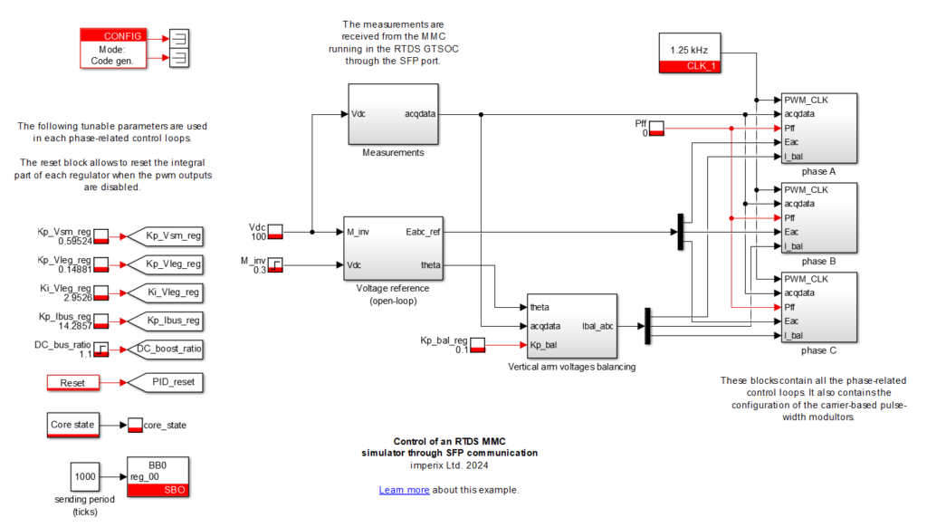
In order to validate the proper communication between the MMC model running on the RTDS GTSOC V2, a simple closed-loop control model – depicted in Fig. 4 – is provided. This model is largely inspired by the AN009, where more information about the operation principles of the MMC converter and controller is available.
From ADC to SBI
Unlike the model from the AN009, measured quantities are not accessed via classical ADC, but rather received from the RTDS simulator through the SFP communication. To achieve a high rate and reduce the CPU load, the reception mechanism is fully handled by the FPGA.
Imperix provides an easy way to transfer data between the CPU and the FPGA: the SBI and SBO registers. As explained in Vivado project section, SBI correspond to FPGA registers that can be read from the CPU, while SBO correspond to FPGA registers that can be written from the CPU.
Once a frame is received, the data is extracted by the driver and automatically routed to SBI registers. To access it from the Simulink model, SBI blocks are instantiated, as shown in Fig. 5. The mapping between the SBI and the received quantities can be found in the SBI mapping section. Also, as quantities are assumed to be received as 16.16 fixed-point data (i.e. it can be configured from the RTDS GTSOC V2), an additional gain of (0.5)^16 is inserted after they are interpreted as integers.

SBI mapping
Data received from the RTDS GTSOC V2 through the SFP communication can be accessed via the following SBI registers. The mapping of the SBI to the received quantities is available here below:
| SBI | Quantity | SBI | Quantity |
| 0:1 | Arm 1, voltage | 18:19 | Arm 4, voltage |
| 2:3 | Arm 1, current | 20:21 | Arm 4, current |
| 4:5 | Arm 1, valves voltage | 22:23 | Arm 4, valves voltage |
| 6:7 | Arm 2, voltage | 24:25 | Arm 5, voltage |
| 8:9 | Arm 2, current | 26:27 | Arm 5, current |
| 10:11 | Arm 2, valves voltage | 28:29 | Arm 5, valves voltage |
| 12:13 | Arm 3, voltage | 30:31 | Arm 6, voltage |
| 14:15 | Arm 3, current | 32:33 | Arm 6, current |
| 16:17 | Arm 3, valves voltage | 34:35 | Arm 6, valves voltage |
| SBI | Quantity | SBI | Quantity |
| 36:47 | Passthroughs 1-3 | 48:59 | Passthroughs 4-6 |
| SBI | Quantity | SBI | Quantity |
| 60:61, 62:63, 64:65, 66:67 | Arm 1, SM voltage: Vsm_A0, Vsm_A1, Vsm_A2, Vsm_A3 | 84:85, 86:87, 88:89, 90:91 | Arm 4, SM voltage: Vsm_B4, Vsm_B5, Vsm_B6, Vsm_B7 |
| 68:69, 70:71, 72:73, 74:75 | Arm 2, SM voltage: Vsm_A4, Vsm_A5, Vsm_A6, Vsm_A7 | 92:93, 94:95, 96:97, 98:99 | Arm 5, SM voltage: Vsm_C0, Vsm_C1, Vsm_C2, Vsm_C3 |
| 76:77, 78:79, 80:81, 82:83 | Arm 3, SM voltage: Vsm_B0, Vsm_B1, Vsm_B2, Vsm_B3 | 100:101, 102:103, 104:105, 106:107 | Arm 6, SM voltage: Vsm_C4, Vsm_C5, Vsm_C6, Vsm_C7 |
| SBI | Quantity | SBI | Quantity |
| 108:111 | Arm 1, SM1-4 status | 120:123 | Arm 4, SM1-4 status |
| 112:115 | Arm 2, SM1-4 status | 124:127 | Arm 5, SM1-4 status |
| 116:119 | Arm 3, SM1-4 status | 128:131 | Arm 6, SM1-4 status |
Note that most of the received quantities are 32-bit wide, which explains why they extend over two 16-bit registers. In particular, voltages and currents are assumed to be encoded as fixed-point 16.16 data. Status are 16-bit words, so each 16-bit SBI register corresponds to one submodule status.
Vivado project
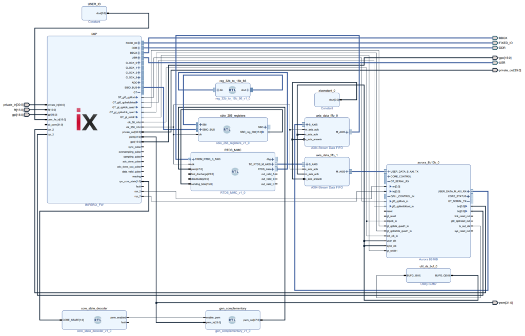
The Vivado block design of the current example is provided below, in Fig. 6. Next sections briefly introduce the main parts of the design, and how to generate the bitstream – running in the B-Box FPGA – from the RTDS_MMC_SFP_gen_script.zip file provided in the Downloads section.
A detailed description of the RTDS MMC driver ports can be found in the driver source file (cf. RTDS_MMC_SFP_gen_script.zip > usr_repo/RTDS_MMC.vhd).
Click here to open as a PDF.
VHDL modules description
| core_state_decoder | Reads the core state and detects if the PWM are enabled by the user in Cockpit. |
| gen_complementary | Spies the PWM signals transmitted to the optical outputs and generates the complementary PWM signals for the RTDS MMC driver. This block can be discarded if the modulators already output complementary PWM signals (configured as ‘dual’ in Simulink/PLECS). Produces a 0-vector if PWM are not enabled. |
| RTDS_MMC | Main driver. Takes the PWM signals as input (along with the optional fast discharge and deactivate signals), builds the 8-bit submodule firing words and transmits them to the RTDS GTSOC V2. It also receives frames from the RTDS GTSOC V2, unpacks them and updates the corresponding registers of the RTDS_data interface. The RTDS_data interface can be extended to directly access any data of interest from the FPGA. Please refer to the RTDS datasheet for more details about the exchanged data. |
| AXI4-Stream FIFO | Used for the clock domain crossing between the main FPGA clock (250MHz) and the Aurora clock domain (50MHz). |
| Aurora 8B/10B | Xilinx Aurora 8B/10B IP. The user manual is available here. |
| reg_32b_to_16b_66 | Splits each 32-bit input (here, 66 inputs) into two 16-bit outputs (here, 132 outputs), to comply with the SBIO registers block 16-bit registers. |
| sbio_256_registers | Extended version (up to 256 registers) of the SBIO registers block. This block contains input registers that can be read from the CPU (SBI), and output registers that can be written from the CPU (SBO). It is therefore used to make the data received from the RTDS available to the CPU. |
How to generate the design and bitstream
The RTDS_MMC_SFP_gen_script.zip folder, provided in the Downloads section above, contains all the necessary files to reproduce the design and generate the bitstream locally. It contains:
- the generation scripts (Batch file, TCL script)
- the source files (VHDL files)
To generate the design using the script, download the RTDS_MMC_SFP_gen_script.zip file and follow the steps described in PN118/Vivado project. Before executing the .bat file, additionally copy the usr_repo folder within the project directory, as shown below:
In Vivado, once the project is ready, click on ‘Generate Bitstream’ to launch the bitstream generation. The warning about the signal size mismatchs can be ignored.
How to assign a different SFP port
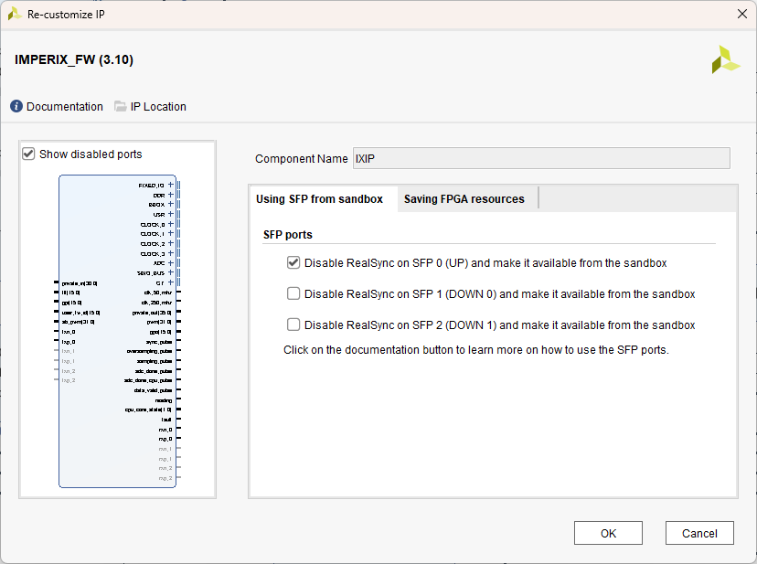
In the provided Vivado project, the SFP communication uses port SFP2 (DOWN 1). To use SFP0 (UP) and/or SFP1 (DOWN 0) instead:
- In the Vivado block design, double-click on the IX IP.
- In the IX IP configuration panel, select options to reflect the desired configuration, as depicted in Fig. 8. Click ‘OK’ to apply the changes. As unconnected tx{p,n} and rx{p,n} IX IP ports could lead to Vivado warnings or issues, note that only the required SFP port(s) must be checked.
- Connect the tx{p,n} and rx{p,n} IX IP port to the corresponding ports of the Aurora IP.
How to change the number of submodules
The RTDS MMC driver provided in the Vivado project is meant to be easily extendable. It however requires minimal experience in FPGA design, typically with Vivado and VHDL basics.
To increase the number of submodules per arm, e.g. to N=12, the following steps are recommended:
- Make sure that the modulator(s) in the controller can produce the Nx6 PWM signals.
- In the following VHDL files, set the N generic to the desired value: RTDS_MMC.vhd, RTDS_rtds_firing_words.vhd, RTDS_emitter.vhd, gen_complementary.vhd. The latter can be discarded if the modulator already outputs the complementary signals.
- Route the PWM signals generated by the modulator to the ‘pwm’ input of the RTDS MMC driver.
If the capacitor voltages and submodule status must be accessed, the following steps are recommended:
- In RTDS_MMC.vhd, add the missing outputs to the RTDS MMC driver (typically, add B_cap_v_sm_XX_leg_X and C_sm_XX_XX_leg_X outputs). Make sure that they are connected to the right serial-to-parallel module.
- In reg_32b_to_16b_66.vhd, extend the module inputs and outputs to match the desired number.
- If necessary, use an SBIO interconnect to instantiate up to 4 SBIO registers blocks and therefore increase the number of available SBIO registers to 1024. The sbio_interconnect.vhd is available in the hdl folder. Add it to the project sources to be able to insert it in the design.
- Do not forget to add the corresponding SBI blocks in the CPU model accordingly.
Additional modifications in the reception mechanism (typ. in RTDS_serial_to_parallel_{B,C}.vhd and RTDS_MMC_router.vhd) are required if the targeted number of submodules exceeds 20.
Going further
As mentioned, this introduction to FPGA-based Aurora communication presents the Aurora 8B/10B protocol and implements an Aurora 8B/10B loopback example.
The page high-level synthesis for FPGA developments shows how automated code generation tools such as Model Composer and Vitis HLS can be used to facilitate the development of FPGA modules. Like the Aurora 8B/10B IP, they use AXI4-Streams to move data around.
The FPGA development on imperix controllers summarizes all the other FPGA-related pages.


