
Table of Contents
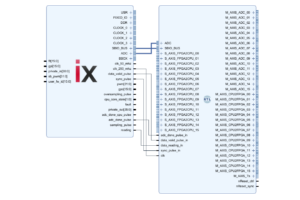
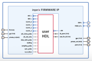
This page documents the imperix firmware IP for AMD/Xilinx Vivado, which is required to program the FPGA of imperix controllers. This IP encapsulates the imperix proprietary FPGA logic and offers various interfaces allowing users to add their own custom logic around it.
The document details the different signals provided by this IP, along with their associated timings. Separate documentation exists for specific interfaces, as listed in the table below:
| Interface | Feature/objective | Product note |
| ADC | Retrieving ADC conversion results as soon as they are available. | PN126 |
| SBIO | Exchanging data between the user code running in the CPU and the FPGA. | PN128 |
| SB-PWM | Driving the PWM output chain, comprised of a dead-time generation system and the hardware protection mechanisms. | PN127 |
| USR | Accessing physical 3V3 I/O pins. | PN179 |
| GT | Accessing Gigabit Transceivers (GT), enabling support of protocols such as Aurora on SFP ports. | PN118 |
| BSCAN | Using ILAs to observe FPGA signals in real-time for debugging purposes. | PN129 |
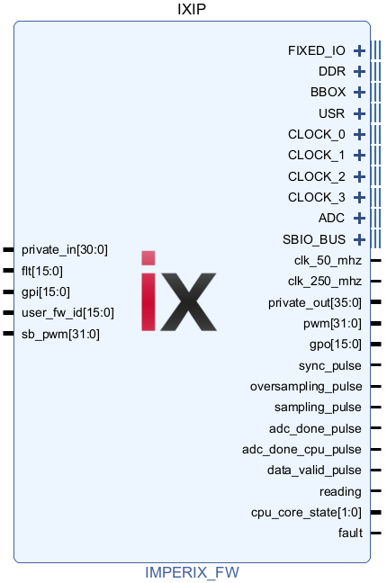
Architecture overview
Because FPGA development operates at the hardware level, a thorough understanding of the underlying system architecture and real-time execution behavior is essential for successfully integrating custom logic into the FPA of an imperix controller.
- The article PN253 presents the architecture of imperix controllers, explains their main data paths, and introduces the key subsystems. Fundamental information regarding how the controllers manage control-relevant clocks and timing is also provided.
- The article PN261 explains how imperix controllers operate and details the typical sequence of acquisition → processing → modulation through the user-programmable CPU. Information is also provided about the core operating states and the related enabling/disabling of PWM outputs.
Imperix actively supports two controller generations, both based on AMD Xilinx System-on-Chips (SoCs):
- Gen 3 controllers (B-Box 3, B-Box Micro, B-Board PRO, TPI8032) are based on an AMD Zynq 7000
- Gen 4 controller (B-Box 4) is based on an AMD Zynq Ultrascale+
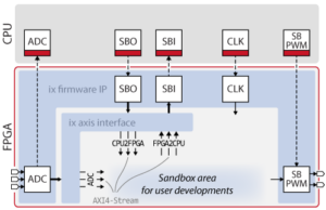
While the specifics (number of CPUs, clock speeds, FPGA resources, etc.) vary between the generations, the operating principles and control workflow are identical. The global architecture is also similar, as shown below:
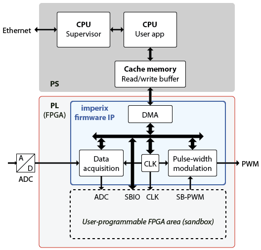
The core modules contained within the imperix firmware IP are:
- The data acquisition module (documented in PN126) pilots the ADC chips and makes the analog input measurement available to both the CPU user app and the user-programmable FPGA area.
- The pulse-width modulation (documented in PN127) contains the pre-implemented PWM modulators (CB, SV, DO, SS, PP). It allows driving the PWM outputs from a custom modulator using the SB-PWM path.
- The CLK module manages the main clock CLK0 (configured via the CONFIG block) and the optional CLK1, CLK2 and CLK3 (configured via CLK block).
- The DMA is responsible for transferring the data between the FPGA and the CPU read/write buffers. The read and write phases are detailed in the next section.
Execution timing & signals
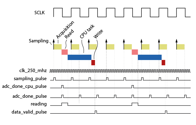
The following figures illustrate the key phases involved along the CPU control path. These are detailed in PN261, and summarized below:
- Acquisition: covers the physical Analog-to-Digital conversion and data retrieval to the FPGA fabric.
- Read: represents the data transfer from the FPGA to the CPU read buffer.
- CPU task: contains the execution of the main control task (user-defined control algorithms).
- Write: represents the data transfer from the CPU write buffer to the FPGA.
Interestingly, a second data path exists, associated with the FPGA task, that permits control algorithms to be fully executed on the FPGA, as in the control example presented in TN147.
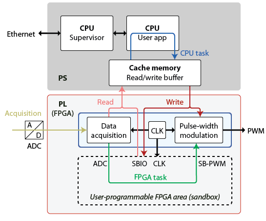
On the PL side (FPGA), the imperix firmware IP provides several signals to monitor and synchronize logic during the execution of these phases.
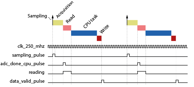
| Port name | Clk domain | Description |
|---|---|---|
| clk_250_mhz | Indicates the ADC sampling instant and the start of the acquisition phase. Corresponds to the rising edge of the sampling clock SCLK. |
| clk_250_mhz | Indicates that the acquisition phase is finished and new ADC values are available at the ADC interface. |
adc_done_cpu_pulse | clk_250_mhz | When the sampling rate differs from the CPU rate, this signal is a decimated version of adc_done_pulse. It is set when the CPU control path stages are scheduled to execute. The following section describes this scenario in more detail. |
| clk_250_mhz | Indicates that the system is in the read phase, in which data flagged as real-time (SBI registers, ADC, GPI, etc.) are sent to the CPU read buffer. |
data_valid_pulse | clk_250_mhz | Asserted at the end of the write phase, notifying that new data were written (SBO registers, PWM duty-cycles, GPO, etc.). |
Handling different execution rates
FPGA-based control algorithms are often desired to execute at a higher rate than the CPU. In such cases, a postscaler can be configured in the CONFIG block to reduce the CPU rate relative to the sampling frequency. Then, the adc_done_cpu_pulse acts as the decimated version of adc_done_pulse. It is asserted when the CPU control path stages are scheduled to run.
Differences between Gen. 3 and Gen. 4 devices
For FPGA development, the B-Box 4 offers several key enhancements over its predecessors, such as access to analog measurements in floating-point format, faster transceivers, and expanded FPGA resources. The table below summarizes the key differences between the two generations.
| Component | Gen 3 | Gen 4 |
| FPGA | Kintex 7 125K | Kintex US+ 504K |
| Logic | LUTs: 78600 Registers: 157200 | LUTs: 230400 Registers: 460800 |
| Logic used by imperix IP* | min: LUTs: 25482 (32.4%) Registers: 46374 (29.5%) max: LUTs: 39143 (49.8%) Registers: 67203 (42.7%) | min: LUTs 70733 (30.7%) Registers 108749 (23.6%) max: LUTs: 94233 (40.9%) Registers: 140636 (30.5%) |
| Usable logic left* | max: LUTs: 53118 (67.6%) Registers: 110826 (70.5%) min: LUTs: 39457 (50.2%) Registers: 89997 (57.3%) | max: LUTs: 159667 (69.3%) Registers: 352051 (76.4%) min: LUTs: 136167 (59.1%) Registers: 320164 (60.5%) |
| Gigabit Transceivers available from the sandbox | 3x GTX (3x SFP connectors) Up to 6.6 Gbps | 4x GTH (1x QSFP connector) Up to 16.3 Gbps |
| Bidirectional direct FPGA I/Os (USR) | 36x | 36x |
| PWM outputs | 32x | 48x |
| ADC interface | 16x (int16) | 24x (int16, or float) |
| RS485/RS422 | – | 2x |
| Acquisition delay | 2 μs (B-Box RCP 3.0) 500 ns (B-Box Micro, B-Board, TPI8032) | 200 ns / 368 ns** |
* The logic used by the imperix IP depends on the enabled features, as explained in the Disabling Features to Save FPGA Resources section.
** When channels A12-A23 are used.
Interface description of the firmware IP
ADC interface
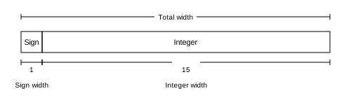
The ADC interface returns the raw 16-bit signed integer result from the ADC chips. Practical guidance for retrieving data from ADCs is provided in PN126.
| Port Name | Direction | Width | Clk domain | Description |
|---|---|---|---|---|
ADC_reg_XX | Output | 16bits | clk_250_mhz | ADC 16-bit result in 2’s complement format. XX = channel |
adc_done_pulse | Output | 1 bit | clk_250_mhz | Indicates that new ADC samples are available. |
adc_done_cpu_pulse | Output | 1 bit | clk_250_mhz | Decimated version of adc_done_pulse when a postscaler is used. Set when the CPU control path stages are scheduled to run. |
ADC_FLOAT interface
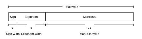
Available exclusively on the B-Box 4, this interface provides access to the true physical values, in single-precision floating-point format, as they are available at the end of the ADC signal chain. The rescaling from the raw 16-bit ADC value is configured by setting the sensor sensitivity and offset from the ADC block.
| Port Name | Direction | Width | Clk domain | Description |
|---|---|---|---|---|
ADC_FLOAT_reg_XX | Output | 32bits | clk_250_mhz | ADC floating-point result post rescaling. XX = channel |
adc_done_float_pulse | Output | 1 bit | clk_250_mhz | Indicates that new ADC_FLOAT samples are available. |
adc_done_cpu_float_pulse | Output | 1 bit | clk_250_mhz | Decimated version of |
SBIO interface
The SBIO_BUS (SandBox IO Bus) is a 16-bit memory-mapped bus allowing the CPU to address up to 1024 registers in the FPGA. This bus is dedicated to user-configured data exchanges between the CPU and the FPGA. Its Simulink/PLECS counterparts are the SBI/SBO blocks. Specific documentation is provided in PN128.
| Port Name | Direction | Width | Clk domain | Description |
|---|---|---|---|---|
SBIO_BUS_sb_addr | Output | 10 bits | clk_250_mhz | Address of the accessed register |
SBIO_BUS_sb_we | Output | 1 bit | clk_250_mhz | Write enable |
SBIO_BUS_sb_wdata | Output | 16 bits | clk_250_mhz | Write data |
SBIO_BUS_sb_rdata | Input | 16 bits | clk_250_mhz | Read data |
The bus performs read operations by setting the requested address on sb_addr and expects the corresponding data on sb_rdata exactly four cycles later.

A write occurs on each rising edge of clk when sb_we is asserted. The target location is given by sb_addr and the value written is sb_wdata.

The two additional signals listed below are provided to help synchronize custom logic with the SBIO bus operations:
| Signal | Direction | Width | Clk domain | Description |
|---|---|---|---|---|
reading | Output | 1 bit | clk_250_mhz | Asserted high while data (ADC, SBI, GPI) are being read by the CPU. |
data_valid_pulse | Output | 1 bit | clk_250_mhz | Single-cycle pulse indicating that all SBO registers have been written for the current CPU control task. |
SB-PWM interface
The SB-PWM (SandBox-PWM) interface allows PWM outputs to be driven from custom FPGA logic while still benefiting from the controller’s hardware protections. Additionally, when using the SB-PWM interface, users also benefit from existing dead-time generation and enable/disable mechanisms similar to driving PWMs from the SB-PWM block (or similar). This interface is further documented in PN127.
| Port Name | Direction | Width | Clk domain | Description |
|---|---|---|---|---|
sb_pwm | Input | 48 bits (Gen 4) 32 bits (Gen 3) | clk_250_mhz | PWM signals driven from sandbox logic. |
CLOCK interfaces
The CLOCK interface provides access to the four user-configurable time clock generators. More information about these resources is provided in PN253. Typical timing configurations are also presented in PN259. On the practical side:
- The main clock CLOCK_0 must be configured via the CONFIG block
- The auxiliary clocks, CLOCK_1, CLOCK_2 and CLOCK_3 must be configured via the CLK blocks.
| Port Name | Direction | Width | Clk domain | Description |
|---|---|---|---|---|
CLOCK_N_period | Output | 16 bits | clk_250_mhz | Period of the clock in ticks. |
CLOCK_N_prescaler | Output | 16 bits | clk_250_mhz | Indicates the CLOCK_N_timer ticking rate.1 tick = 4 ns * |
CLOCK_N_timer | Output | 16 bits | clk_250_mhz | Timer counting from 0 to CLOCK_period-1 at the ticking rate set by the CLOCK_N_prescaler. |
CLOCK_N_clk_en | Output | 1 bit | clk_250_mhz | Clock enable pulse indicating when CLOCK_N_timer is updated. |
Interestingly, the prescaler extends the achievable frequency range beyond what the 16-bit period timer counter alone can provide. With CLOCK_N_prescaler = 1, the minimum achievable frequency is approximately 3.8 kHz (250 MHz / 65535). For lower frequencies, the CLOCK_N_prescaler automatically increases, and the firmware tries to closely match the requested frequencies.
Example:
- A frequency of 20 kHz results in
CLOCK_prescaler = 1andCLOCK_period = 12500 ticks. - A frequency of 2 kHz results in
CLOCK_prescaler = 2andCLOCK_period = 62500 ticks.
When prescaler = 1:
clk_enis asserted everyclk_250_mhzcycleCLOCK_0_timerincrements on every clock edge

When prescaler > 1:
clk_enis asserted once every X cycles (where X = prescaler value)CLOCK_0_timerincrements only whenclk_enis high

GT interfaces
The Gigabit Transceiver (GT) interface provides access to high-speed serial transceivers connected to the SFP+, respectively QSFP+ sockets. This enables custom point-to-point communication with external devices such as other controllers, custom hardware etc.
PN118 is an example setting up loopback communication using Xilinx/AMD Aurora as a communication protocol. Additional examples with third-party hardware-in-the-loop (HIL) simulators (OPAL-RT, Plexim and RTDS) are provided on the page SFP communication with third-party devices.
| Feature | Gen 4 | Gen 3 |
|---|---|---|
| Available transceivers | 4x GTH (1x QSFP connector, lanes 4–7) | 3x GTX (3x SFP connectors) |
| Maximum line rate | 16.3 Gbps | 6.6 Gbps |
Accessing GTH transceivers on Gen 4 controller
On Gen 4, lanes can be exposed to the sandbox from the Configuration tab in the imperix firmware IP configuration. Each enabled lane exposes the following signals:
| Port Name | Direction | Description |
|---|---|---|
GT_USER_TX_N_txp | Output | Transmit positive (differential) |
GT_USER_TX_N_txn | Output | Transmit negative (differential) |
GT_USER_RX_N_rxp | Input | Receive positive (differential) |
GT_USER_RX_N_rxn | Input | Receive negative (differential) |
gt_refclk | Output | 250 MHz reference clock (shared across all lanes) |
Accessing GTX transceivers on Gen 3 controller
On Gen 3, the SFP ports are used by default for RealSync inter-device communication. Using a port from the sandbox requires disabling RealSync on that specific link, which removes the inter-device communication capability on that port. Lanes can be exposed to the sandbox from the Configuration tab in the imperix firmware IP configuration. Each enabled lane exposes the following signals:
| Port Name | Direction | Description |
|---|---|---|
txp_N | Output | Transmit positive (differential) |
txn_N | Output | Transmit negative (differential) |
rxp_N | Input | Receive positive (differential) |
rxn_N | Input | Receive negative (differential) |
Serial port interfaces
The serial port interfaces are exclusive to the B-Box 4 and are typically used by the pre-implemented SSI, BiSS-C and EnDat2.2 FPGA drivers. The imperix IP allows bypassing these built-in drivers by providing direct access to RS485/RS422 transceiver signals from the sandbox, as illustrated below.
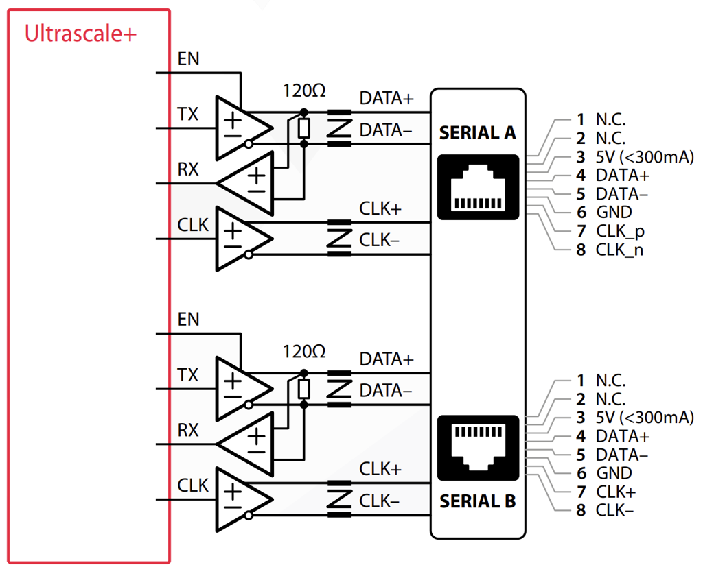
The serial ports (A and/or B) can be made available from the sandbox from the Configuration tab in the imperix firmware IP configuration. Each enabled serial port exposes the following signals:
| Port Name | Direction | Description |
|---|---|---|
SERIAL_X_rx | Input | Receive data from external device |
SERIAL_X_tx | Output | Transmit data to external device |
SERIAL_X_clk | Output | Clock signal for synchronous protocols |
SERIAL_X_en | Output | Transceiver enable (active high) |
BSCAN Interface to observe internal signals using ILA
The BSCAN (Boundary Scan) interface exposes the FPGA’s debug scan chain to the sandbox and enables the use of Integrated Logic Analyzers (ILAs) and other Xilinx debug cores. When combined with the Xilinx Virtual Cable (XVC) protocol, this allows remote debugging of internal FPGA signals directly from Vivado’s Hardware Manager over Ethernet.
For detailed instructions on adding ILAs to your design and connecting to them via XVC, refer to PN129.
Digital I/Os drivers
The sandbox exposes various digital I/O signals. Some ports are available for user logic, while others are reserved for internal system operation and must not be modified. For detailed pin locations and electrical specifications, refer to the relevant datasheet:
- B-Box 4 datasheet
- B-Box RCP datasheet
- B-Box Micro datasheet
- B-Board PRO datasheet
- TPI 8032 datasheet
The USR pins
The USR pins are 36 user-configurable 3.3V I/Os routed directly to the FPGA, without any resistors or level shifters on the PCB traces. These pins are typically used for interfacing external peripherals (e.g., SPI ADC) but can, in fact, be leveraged for a very broad range of applications, thanks to their bidirectionality and high bandwidth.
More information about accessing USR pins is provided in PN179.
| Port Name | Direction | Description |
|---|---|---|
USR[35:0] | Tristate | These pins are used by the motor interface and the programmable inverter. When none of these devices are in use, the USR pins can freely be accessed from the sandbox. |
Private Ports
These ports are required for internal communication with controller components and are reserved for imperix use. Modifying these connections may cause undefined behavior and must be absolutely avoided.
| Port Name | Direction | Description |
|---|---|---|
private_in | Input | Internal system signals. Width varies by generation. |
private_out | Output | Internal system signals. Width varies by generation. |
DDR | – | DDR memory interface |
FIXED_IO | – | Fixed I/O interface to PS |
Gen 4 ports
| Port Name | Direction | Description |
|---|---|---|
din[23:0] | Input | General-purpose or fault feedback inputs (GPI/FLT) |
dout[47:0] | Output | General-purpose outputs or PWM outputs (GPO/PWM) |
dout connection, as this would bypass the protection mechanism! Instead, PWM signals should always be routed through the sb_pwm input port.Gen 3 ports
| Port Name | Direction | Clock Domain | Description |
|---|---|---|---|
flt[15:0] | Input | clk_250_mhz | Fault inputs |
gpi[15:0] | Input | clk_250_mhz | General-purpose inputs |
gpo[15:0] | Output | clk_250_mhz | General-purpose outputs |
pwm[31:0] | Output | clk_250_mhz | PWM output signals |
BBOX[51:0] | Tristate | N/A | Internal B-Box RCP pins. Can be repurposed on B-Board PRO with custom PCB design (see PN201). |
dout connection, as this would bypass the protection mechanism! Instead, PWM signals should always be routed through the sb_pwm input port.Disabling features to save FPGA resources
The imperix firmware IP includes several optional features that can be disabled to free up FPGA resources for custom sandbox logic. Access the resource-saving options from the Saving FPGA resources tab in the imperix firmware IP configuration.
Disabling a feature removes it entirely from the FPGA design. If the corresponding functionality is used in the CPU model, an error will be raised in Cockpit. Additionally, unused modulators can be removed to save logic resources. Notably, the CB-PWM logic can be disabled in groups of 8 lanes.
| Feature | Gen 4 | Gen 3 |
|---|---|---|
| CB-PWM lanes 0–7 | ✓ | ✓ |
| CB-PWM lanes 8–15 | ✓ | ✓ |
| CB-PWM lanes 16–23 | ✓ | ✓ |
| CB-PWM lanes 24–31 | ✓ | ✓ |
| CB-PWM lanes 32–39 | ✓ | — |
| CB-PWM lanes 40–47 | ✓ | — |
| SS-PWM logic | ✓ | ✓ |
| PP-PWM logic | ✓ | ✓ |
Resource Savings
| Feature | Gen 4 | Gen 3 |
|---|---|---|
| CB-PWM (per 8 lanes) | ~2100 LUTs (0.9%) ~2800 Registers (0.6%) | ~1600 LUTs (2.03%) ~2000 Registers (1.27%) |
| SS-PWM | ~6250 LUTs (2.71%) ~5500 Registers (11.93%) | ~2700 LUTs (3.43%) ~3300 Registers (2.1%) |
| PP-PWM | ~4400 LUTs (1.9%) ~9200 Registers (2%) | ~4400 LUTs (5.6%) ~9150 Registers (5.82%) |
Related Articles
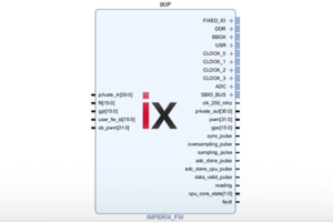
Download of the imperix firmware IP for FPGA sandbox

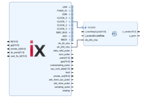
Driving PWM outputs from the FPGA

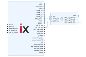
Exchanging data between the CPU and the FPGA
Getting started with FPGA programming
Retrieving ADC measurements from the FPGA
Upgrading the imperix firmware IP