Table of Contents
This page explains how to get started with the modular multilevel converter (MMC) bundle configured as a 9-level, 3-phase inverter. It provides a comprehensive overview of the hardware configuration and step-by-step instructions to commission the equipment.
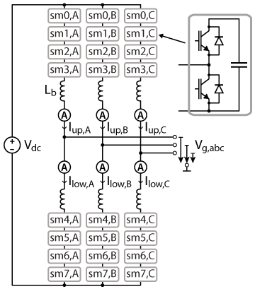
This page focuses on the basic commissioning of the default configuration of the MMC bundle, which is a 3-phase inverter containing 24 half-bridge submodules (Figure 1). For the sake of simplicity, the proposed commissioning plan uses an open-loop approach with Sort-&-Select balancing. This PWM-based modulation scheme inherently handles the balancing of the submodule voltages by sorting them and then selecting which module should be inserted or bypassed first. For more details on the implementation of the Sort-&-Select modulation, please refer to the technical note SS-PWM. Alternatively, a more advanced balancing strategy controlling all state variables is detailed in the technical note TN153.
Setting up the MMC bundle
The content of the MMC bundle, listed below, includes all the components needed for the realization of a 9-level, 3-phase inverter with 24 submodules.
- 2x programmable controller (B-Box 4)– see Quick-start guide
- ACG SDK toolbox for automated generation of the controller code from Simulink or PLECS
- 3x power racks (type B)
- 24x full-bridge modules (PEH2015)
- 1x grid connection panel with switchgear and precharge circuit
- 4x voltage sensors
- 6x current sensors
- All necessary RJ45 and fiber optic cables
On top of that, some additional material, listed below, is required to test the system before operating the full converter.
- Laboratory DC power supply (rated for at least 100V, 5A)
- 3x power resistors (5-100Ω) to emulate a load at the grid terminal
Wiring of the power and control stages
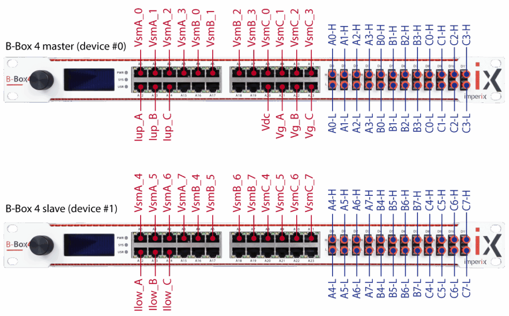
Per default, in the MMC bundle, the full-bridge modules PEH2015 are wired in such a way that only one half-bridge is used. This way, two B-Box 4 suffice to drive the 48 switches of the MMC (24 optical PWM outputs per B-Box 4).
While the master B-Box 4 (device #0) runs the control for all 6 arms, it only interfaces with the 3 upper arms. On the other hand, the slave (device #1) acts as an I/O extension to the 3 lower arms. As such, the CPU in the slave B-Box 4 does not run any user code; only its FPGA is active (see Distributed Converter Control for more details).
The wiring of the RJ45 analog signal cables (red) and the optical PWM gate signals (blue) for the two B-Box 4 is shown in Figure 2 below.
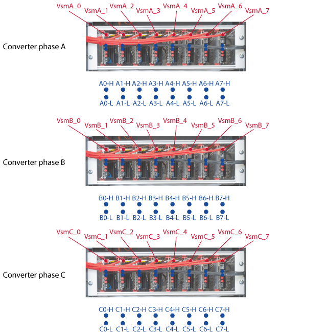
The counterpart of the wiring on the power racks is depicted in Figure 3.
On the rear side of the cabinet, the power terminals, the grid connection panel, and the external voltage and current sensors are wired as shown in Figure 4.
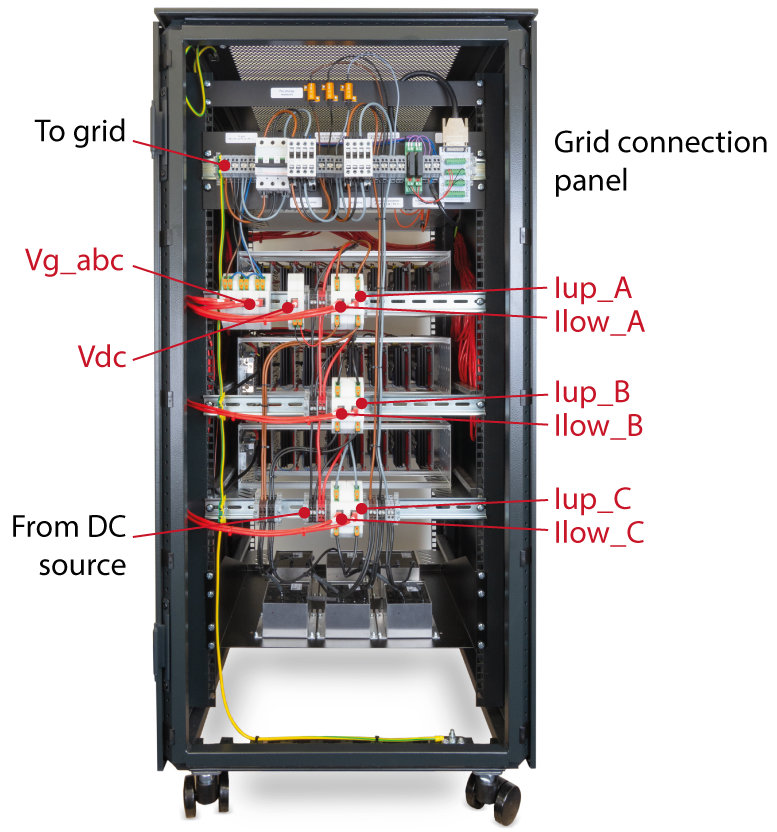
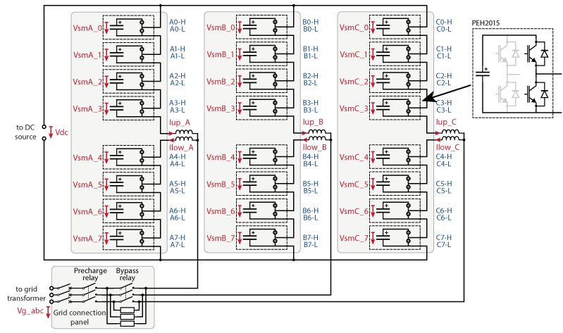
Figure 5 gives a comprehensive overview of the electrical wiring as well as the naming of the measured signals and PWM gate signals.
Configuration of the analog input protections
To ensure that the ratings of the power converter are never exceeded, the analog input protection limits of the B-Box 4 must be configured properly. A detailed explanation of how to compute these limits for B-Box 4 is given in PN252. Additional details on over-current and over-voltage protection can be found in PN257.
| Measured signal | Range (SI units) | Sensor type | Input channel number | Limit high [V] | Limit low [V] | Reaction time |
|---|---|---|---|---|---|---|
| \(V_{sm,(A,B,C),0…7}\) | 0…215V | PEH2015 voltage | 0…11 | 1.9 | -1.9 | fast |
| \(I_{up,(A,B,C)}\) (only on master B-Box) | -15…15A | CSR-25-HBW | 12…14 | 3.0 | -3.0 | fast |
| \(I_{low,(A,B,C)}\) (only on slave B-Box) | -15…15A | CSR-25-HBW | 12…14 | 3.0 | -3.0 | fast |
| \(V_{g,(A,B,C)}\) (only on master B-Box) | -340…340V | VSR-1000-ISO | 21…23 | 1.7 | -1.7 | fast |
| \(V_{dc}\) (only on master B-Box) | 0…800 V | VSR-1000-ISO | 20 | 4.0 | -4.0 | fast |
When using B-Box 4 controllers with the CSR-25-HBW and VSR-1000-ISO sensors, the configuration is made easier thanks to sensor auto-identification (see PN255).
Commissioning the MMC bundle
Before operating the system, it is always a good idea to test that everything is properly wired and configured. With the help of the Simulink (or PLECS) model below, the following test procedure can be used to check the behavior of the MMC bundle wired as a 9-level, 3-phase inverter.
These basic models are designed to operate the MMC converter as an open-loop voltage-source inverter. The ADC blocks retrieve the analog measurements for monitoring. The selected sampling technique is synchronous averaging (see PN258: Advanced sampling techniques for power electronics). The SS-PWM blocks implement the Sort-&-Select balancing algorithm in each arm individually. The relays of the grid-side panel are operated directly with tunable parameters.
Test procedure
A simple way to test an inverter is to operate it in open-loop mode on a passive load. A DC power supply is connected to the DC input and three resistors in a star configuration are connected on the AC side of the converter, as shown in Figure 7 below.
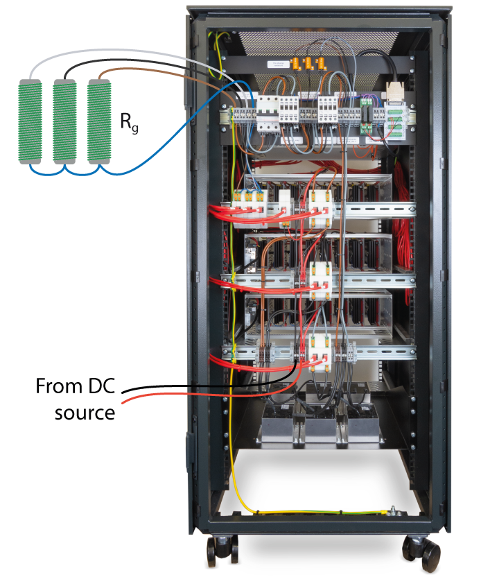
Sizing of the load resistors
The theoretical RMS current can be computed as
$$I_{g,rms}=\frac{\sqrt 2\cdot V_{dc} \cdot M_{inv}}{2\cdot R_g}$$
where \(V_{dc}\) is the DC input voltage, \(M_{inv}\) the modulation depth of the inverter (tunable parameter M_inv) and \(R_g\) the resistance of the load.
In this guide, \(R_g\) is chosen as \(8.5\,\Omega\), \(M_{inv}=0.3\) and \(V_{dc}=200 \,\text{V}\). This results in an RMS current of \(5\,\text{A}\) through the resistors, which is within the rated current of the selected resistors (\(13.5\,\text{A}\)).
If the rating of the resistor is exceeded, the DC supply voltage and/or the modulation depth of the inverter can be reduced accordingly.
Loading the code and setting up the workspace in Cockpit
- In Simulink:
- Open the Simulink model and set the mode to Automated Code Generation in the CONFIG block.
- Build the model (Ctrl + B). It will automatically launch Cockpit.
- Or in PLECS:
- Open the PLECS model.
- Open the coder options (Ctrl + Alt + B) and click Build in the bottom right. It will automatically launch Cockpit.
- In Cockpit:
- Set the target IP in Cockpit and click on Create to generate a new project.
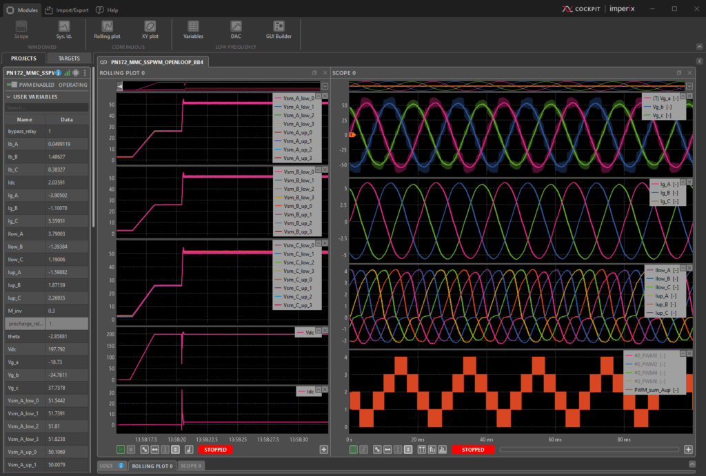
- Add a new rolling plot module. Click four times on the “+” icon in the bottom right such as to see 5 sub-plots. Drag-&-drop the variables
VsmA_0toVsmA_7into the 1st sub-plot, the variablesVsmB_0toVsmB_7into the 2nd sub-plot andVsmC_0toVsmC_7into the 3rd. The input voltageVdccan be drag-&-dropped to the 4th sub-plot and the input currentIdcto the 5th. - Add a new scope module. Click twice on the “+” icon on the bottom right of the scope to add 2 additional sub-plots to the scope. Drag-&-drop the grid grid voltages
Vg_a,Vg_bandVg_cto the 1st sub-plot and the grid currentsIg_a,Ig_bandIg_cto the 2nd sub-plot. The 3rd sub-plot can be used to monitor the inductor voltagesIlow_A,Ilow_B,Ilow_C,Iup_A,Iup_BandIup_C. - With B-Box 4 controllers, it is possible to visualize the PWM signals generated by the modulator. To do so, add a 4th plot to the scope module by pressing the “+” icon on the bottom right, and add the following PWM signals from the variable panel under the PWM section:
#PWM_0,#PWM_2,#PWM_4, and#PWM_6. The formula builder can then be used to reconstruct the modulated voltage on the upper arm in phase A by adding the formulaPWM_sum_Aup = #PWM_0 + #PWM_2 + #PWM_4 + #PWM_6.
Step-by-step test procedure
Before powering up the system, ensure you are familiar with the safety rules for working with electrical power equipment. Basic rules are reminded in this article: TN181: Safety recommendations for working in the lab.
- Gradually increase the voltage of the DC source from 0V to 200V (or to the voltage chosen in the sizing of the resistors).
- Verify that the measured input voltage
Vdcmatches the voltage of the source. - Verify that the sub-modules get charged to one eighth of the input voltage (25V in the presented example).
- Manually close the breaker on the grid-side panel and close the relays by setting the variables
bypass_relayandprecharge_relayto 1 in the variable list on the left-hand side in Cockpit. - Enable the PWM pulses by toggling the PWM switch at the top left corner in Cockpit.
- Verify that the sub-module capacitor voltages jump to one fourth of the input voltage (50V in the presented example).
- The grid voltages should have a sinusoidal form with a theoretical amplitude
$$\langle\hat{V_g}\rangle=M_{inv}\cdot V_{dc}\ \ \ (\approx 60\,\text{V}).$$ - The grid currents should have a sinusoidal form with a theoretical amplitude
$$\langle\hat{I_g}\rangle=\frac{M_{inv}\cdot V_{dc}}{R_g}\ \ \ (\approx 7\,\text{A}).$$ - The current drawn from the DC source should theoretically be
$$I_{dc}=\frac{3}{2}\cdot\frac{M_{inv}^2\cdot V_{dc}}{R_g}\ \ \ (\approx 3\,\text{A}).$$ - Reduce the input voltage to 0V and observe the discharging of the sub-module capacitors.
- Disable the PWM.
The screenshot below shows what the workspace could look like in the end, while running the test procedure.
To go further…
With the basic functionality of the equipment tested, one could dive deeper into the control strategy for the MMC, including its connection to the grid: Three-phase MMC converter. Another application using the MMC bundle is presented in MMC-based audio amplifier.
Other examples with modular multi-level topologies include the cascaded H-bridge (TN165), which can be applied, for instance, in STATCOMs (AN013) and solid-state transformers (AN015).