Table of Contents
Solid-state transformers (SST) are AC-AC power electronic converters featuring medium-frequency (MF) isolation transformers and present an alternative to conventional low-frequency (LF) transformers. The main advantages of SSTs over LF transformers are their size and weight, which are considerably reduced thanks to the increase of the fundamental frequency in the isolation transformer(s). Moreover, modern power electronics and digital control technologies make possible the application of SSTs in future medium-voltage (MV) distribution smart grids, where modularity and controllability are key elements. [1,2]
This article briefly describes a control strategy for a selected SST topology and presents its experimental validation on a prototype using imperix hardware and software.
Converter topology
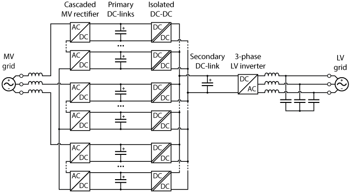
A typical modular SST topology was studied in [3], where a cascaded topology is used at the MV side to withstand the MV voltage level. The galvanic isolation is ensured by isolated medium-frequency DC-DC converters, whose secondary DC terminals are connected in parallel to a low-voltage (LV) 3-phase inverter.
Control implementation of the solid-state transformer
As opposed to conventional LF transformers, the use of power electronics in SSTs makes possible the control of the active and reactive power flows, which is essential in smart grid applications [2]. As explained in TN169, the reactive power flow is linked to the voltage amplitude at the nodes in the grid, while the active power flow is related to the grid frequency and the voltage phase shift between the nodes. For these reasons, the control objectives have been defined as:
- Reactive power flow in the MV grid (A),
- Voltage amplitude in the LV grid (B),
- LV grid frequency (C),
- Phase shift between the MV and LV grid voltages (D).
Additionally, the following low-level control objectives are necessary for the stable operation of the converter:
- Control and balancing of the primary (MV) DC-link voltages (E),
- Control of the secondary (LV) DC-link voltage (F).
Main control subsystems
This section describes the control architecture implemented to achieve the control objectives listed above. The main subsystems are the control of the cascaded H-bridge, the dual active bridge, and the 3-phase LV inverter.
The cascaded topology of the MV rectifier is implemented as a cascaded H-bridge, whose control strategy is detailed in TN165. The control of the cascaded H-bridge is responsible for the regulation and balancing of the primary DC-link voltages (control objective E: Vdc,prim,ref) and it allows tracking a reactive power reference at the MV grid terminals (control objective A: QMV,ref). As such, the implemented control is similar to the one of a static synchronous compensator (STATCOM, see AN013).
The isolated DC-DC converters are based on the dual active bridge (DAB) topology and are controlled using phase-shift modulation, as detailed in TN115. Since they share a common secondary DC-link (all connected in parallel), only one voltage must be regulated and thus only one voltage controller is needed (control objective F: Vdc,sec,ref). For this purpose, the voltage controller proposed in TN115 has been slightly modified to evenly split the transferred power between the DAB stages.
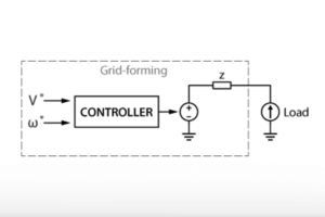
In the present control example, the 3-phase LV inverter is implemented as a grid-forming inverter (TN168). The d-axis voltage reference is set to the desired LV voltage amplitude (control objective B: Vac,LV,ref) and the q-axis voltage reference is set to 0. The angle of the dq reference frame can either be taken from the PLL of the MV rectifier by adding a freely choosable phase shift (control objective D: phaseShiftMV,LV) or generated with an independent frequency (control objective C: fLV).
Operation logic
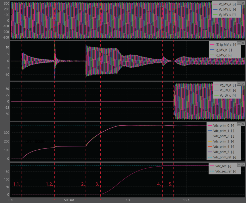
To operate the converter starting with discharged capacitors, a proper start-up sequence must be implemented to avoid high inrush currents that could potentially cause damage. The steps are described hereafter and illustrated in Figure 5.
- Precharge of the primary DC-links from the MV grid via precharge resistors (see TN131):
- Closing of the precharge contactor,
- Closing of the bypass contactor;
- Activation of the cascaded H-bridges (voltage control of the primary DC-links);
- Soft-start of the DAB converters (see TN115);
- Activation of the DAB voltage controller (secondary DC-link voltage control);
- Activation of the LV grid-forming inverter.
For a safe and fast de-energizing of the system, an active discharge sequence has been implemented. It relies on a resistive load connected to the LV grid, in which the energy is dissipated. The steps of the active discharge sequence are the following:
- Deactivation of the cascaded H-bridge: the primary DC-link voltage control is deactivated and the converter is disconnected from the MV grid via contactor opening,
- Deactivation of the DAB secondary sides: the secondary DC-link voltage control is deactivated and the secondary sides of the DAB act as passive diode rectifiers,
- The grid-forming inverter still tries to maintain the LV grid voltages,
- The energy stored in the DC-link capacitors is dissipated in the load on the LV grid side.
- When all DC-link voltages are below a pre-defined voltage threshold (e.g. 5V), all PWM signals are deactivated.
Scaled-down prototype of a solid-state transformer
Topology
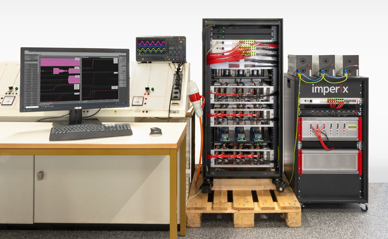
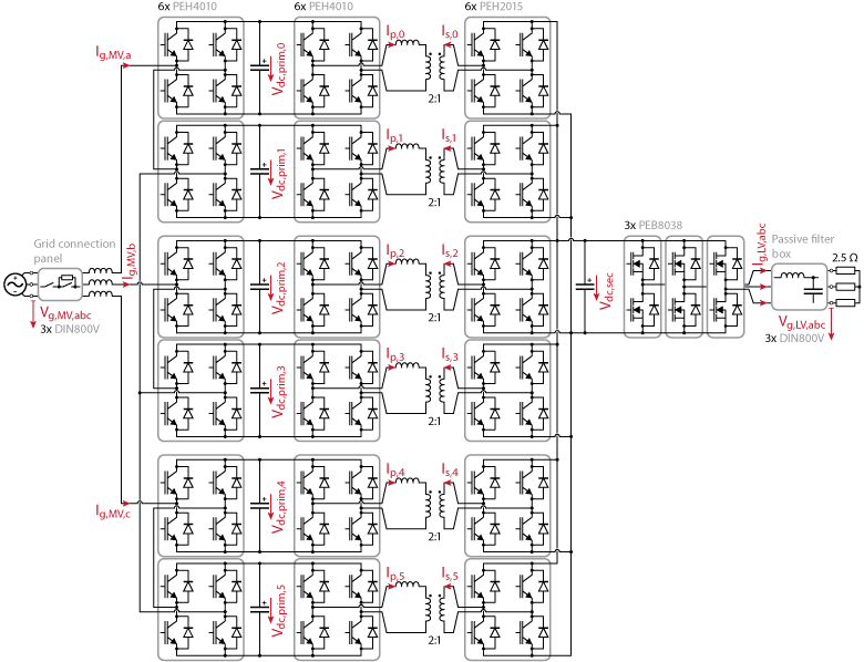
The control example is validated on a prototype containing 6 cascaded H-bridges (2 per phase). For a safe connection to the grid, the MV side is connected via a grid connection panel to the 230V/400V 50Hz grid. The cascaded H-bridges and the primary sides of the DAB converters are implemented using PEH4010 full-bridge IGBT modules, the secondary sides of the DAB using PEH2015 full-bridge IGBT modules, and the LV grid-forming inverter using PEB8038 half-bridge SiC modules. On the LV side, an LC filter is implemented using a passive filter box and a 2.5 Ω resistive load is connected in star configuration. The measurements are taken from the built-in voltage and current sensors of the power modules, except for the MV and LV grid voltages, which are measured using external DIN800V voltage sensors.
Experimental results
To use all the voltage levels of the cascaded H-bridge with a 230V/400V grid at the MV terminals, the primary DC-link voltage reference Vdc,prim,ref is set to 200 V. Due to the 2:1 turns ratio of the DAB transformers, the secondary DC-link voltage reference Vdc,sec is set to 100 V. For an overall transformation factor for the solid-state transformer of 10:1, the voltage of the LV grid is chosen as 23 Vrms (Vac,LV,ref is set to 32,5 V).
In Figure 7, the switched line-to-line MV and LV voltage waveforms are shown together with the MV and LV grid currents to validate the correct switching of the MV cascaded H-bridge and the LV grid-forming inverter. In this test, the reactive power reference QMV,ref and the phase shift between the MV and LV voltages are both set to 0.
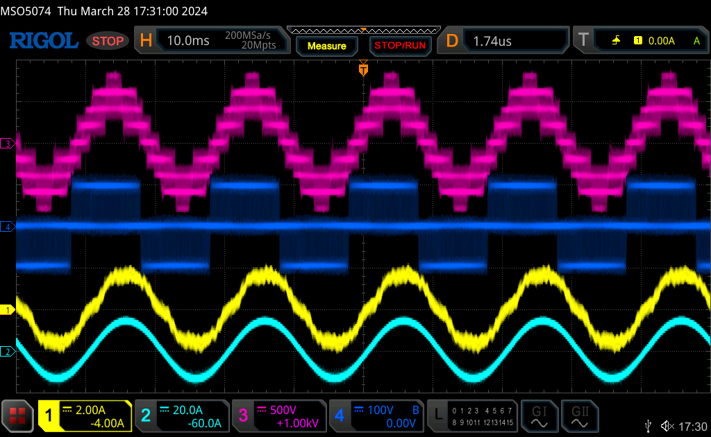
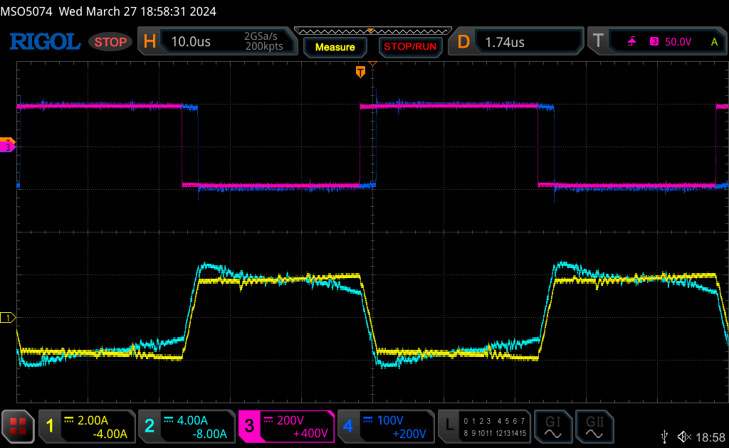
The voltage and current waveforms for one of the DAB converters are shown in Figure 8. The phase shift between the primary and secondary switched voltages can easily be seen.
Downloads
Two sets of files are proposed, suitable for implementing the control and simulating its behavior in MATLAB Simulink or Plexim PLECS environment.
Imperix Power library requires ACG SDK 2024.2 or a later version. To update the ACG SDK, please go to imperix.com/downloads/.
Simulink model
PLECS model
Minimum requirements:
- Imperix ACG SDK 2024.2 or newer.
- For control code development and simulation in Simulink:
- MATLAB Simulink R2016a or newer
- For control code development and simulation in PLECS:
- Plexim PLECS 4.5 or newer.
Academic references
[1] W. McMurray, “Power converter circuits having a high frequency link,” U.S. Patent 3 517 300, June 23, 1970.
[2] J. Huber, J. W. Kolar, “Solid-State Transformers – On the Origins and Evolution of Key Concepts,” in IEEE Industrial Electronics Magazine, pp. 19-28, September 2016.
[3] J. Huber, J. W. Kolar, “Applicability of Solid-State Transformers in Today’s and Future Distribution Grids,” in IEEE Industrial Electronics Magazine, pp. 19-28, September 2016.


