Table of Contents
The DC transmission systems are widely used in DC grids, rail transit systems, and electric vehicle charging systems. In these applications, the DC supply can reach several kilovolts, and the input voltage can be relatively high with respect to the output voltage. Therefore, modular DC-DC converters connected in series at the input and in parallel at the output are employed. Compared to the use of a single DC-DC converter, this configuration helps reduce the voltage stress on the switching devices as the voltage and current are shared among multiple converter modules. Additionally, it offers other advantages such as reduced cost and manufacturing effort, as well as improved power density and scalability [1, 2]. Among the various topologies discussed in the literature, the input-series output-parallel dual active bridge (ISOP DAB) is widely adopted.
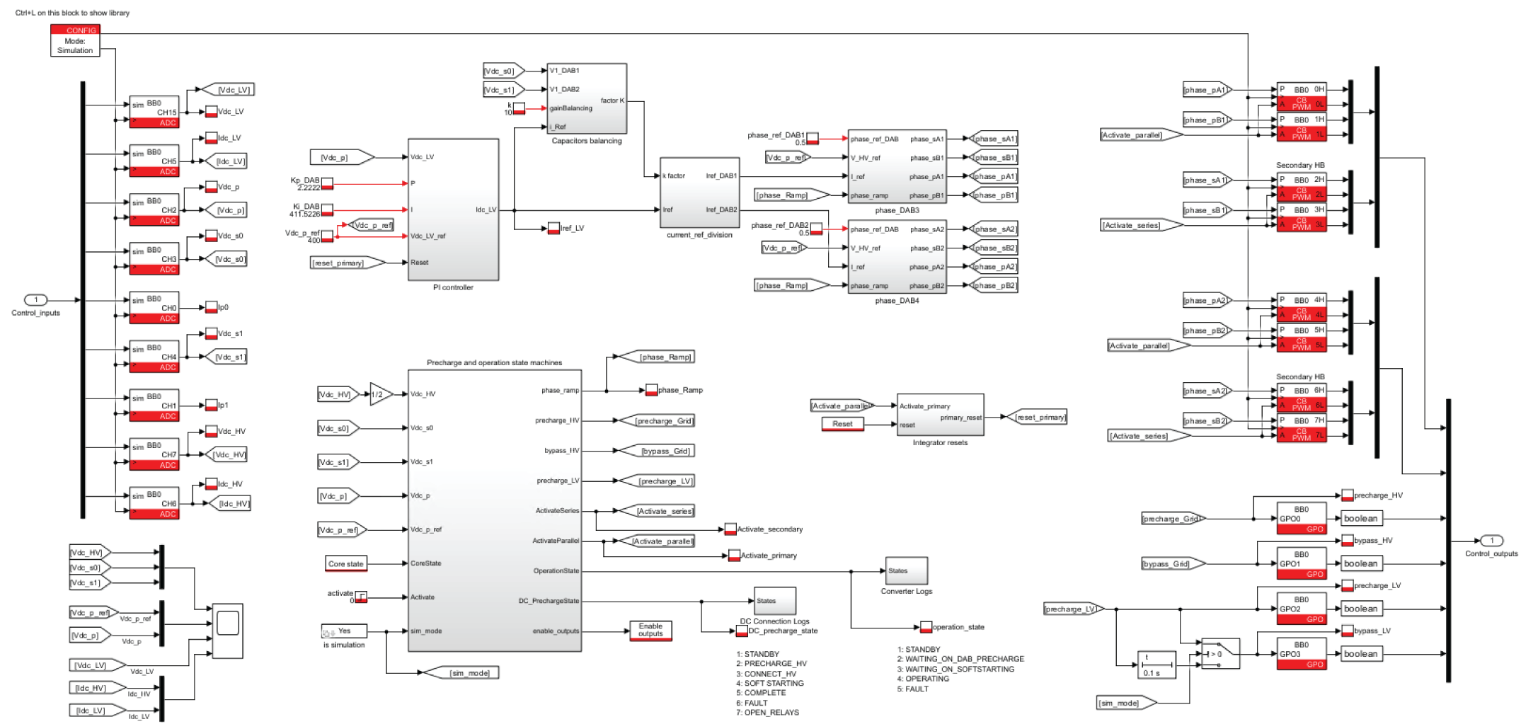
In this technical note, a control strategy for an ISOP DAB system formed by two modules is presented. The ISOP DAB topology is explained in detail followed by a summary of the existing control strategies. After that, the selected approach is explained, the experimental implementation on the B-Box RCP is introduced using ACG SDK on Simulink, and experimental results are shown.
More information regarding the DAB modulation techniques can be found in TN116. Additionally, in TN115, the control implementation of a DAB using phase-shift modulation is carried out, where the soft-start of the DAB is also explained.
Topology of the 2×2 ISOP DAB
The ISOP DAB system consists of multiple DAB modules connected in series at the input and in parallel at the output. Each DAB module is generally a bidirectional DC-DC converter composed of two identical full-bridge circuits connected through a transformer on the AC side. This topology enables high voltage conversion efficiency by achieving zero-voltage switching (ZVS), which is realized by controlling the phase-shift between the input and output bridges, thereby reducing switching losses. Additionally, the transformer provides galvanic isolation, preventing faults on one side from propagating to the other. Finally, it also offers soft start capability through gradual phase-shift control, which starts from zero and increases smoothly, avoiding sudden spikes in voltage or current [2].
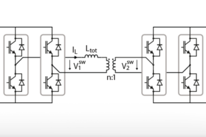
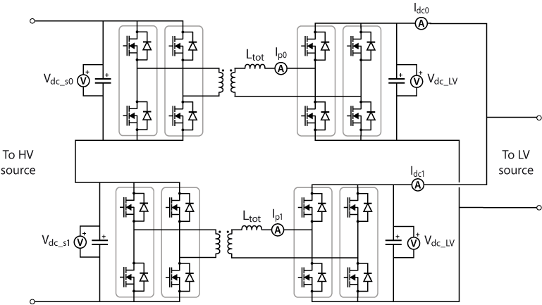
In this technical note, two modules have been used to implement the ISOP DAB system. The schematic is represented in Fig. 1, where the leakage inductance and any additional inductance placed at the series or at the parallel sides are represented by the inductor \(L_{tot}\). Additionally, the subscripts s and p refer to the series- and parallel-connected sides, respectively.
Control strategy
In an ISOP DAB system, it is important to ensure power balance between the DAB modules; that is, both the input voltage and output current must be evenly shared. Directly controlling the output currents can lead to instability, because adjusting the phase shift of one module changes its power transfer, causing the input-capacitor voltages to deviate from their nominal values and affecting the other modules’ operating points. In contrast, controlling the input voltages provides a stable and effective power balancing. By regulating the input voltages, each module delivers approximately constant power, ensuring that the output power of all modules is nearly equal. At steady state, balanced input voltages correspond to nearly equal output currents, and vice versa [1].
To achieve balanced power transmission, various control strategies have been proposed in the literature. One commonly used approach is the three-loop control method [1, 2], which is applied to ISOP DAB systems with N modules. This method typically consists of an outer loop for the output voltage regulation, an inner loop for input voltage sharing, and a current control loop for each module. However, for ISOP DAB systems with only two modules, simpler strategies using fewer controllers can be adopted. In such a case, a feed-forward control method can be employed to maintain power balance [3]. This method regulates the output current distribution between the DAB modules, which eventually also equalizes the input voltages.
As in this technical note a two-module ISOP DAB system is used, the feed-forward control method has been implemented for simplicity, even if the three-loop control method [1, 2] could be applied as well. The feed-forward control scheme is illustrated in Fig. 2, where \(V^{*}_{dc\_LV}\) represents the desired reference at the output, \(\phi_0\) and \(\phi_1\) are the phase-shift of each DAB and \(k\) is the balancing factor.
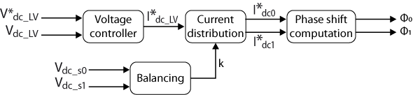
As it can be observed, the control scheme consists of four main blocks: a voltage controller, a current distribution stage, a balancing stage, and the calculation of the phase-shift. Each block is detailed below.
Voltage controller
The voltage controller regulates the output voltage of the DABs. Since the outputs are connected in parallel, both DABs share the same output voltage. The controller’s block diagram is shown below and includes a typical PI controller designed using the Symmetrical Optimum method. The controller’s output determines the total current flowing through the LV side, which must be distributed between the two DABs to ensure balanced input voltages.

Balancing factor
The balancing factor, \(k\), is calculated so the input voltages of the DABs stay equally balanced [3]. It must be inside the range \([0,1]\) and is given by:
$$ (1)\quad k = 0.5 + K\left(\frac{V_{dc\_s0}-V_{dc\_s1}}{V_{dc\_s0}+V_{dc\_s1}}\right)\mathrm{sign}(I^*_{dc\_LV})$$
where \(K\) is a gain that adjusts the amount of balancing, either increasing or decreasing its effect. This gain is chosen empirically and should guarantee convergence to steady-state conditions while ensuring effective correction of any voltage or power imbalance. The sign of the current allows reversing the effect of the voltage difference based on the direction of the current, ensuring that the voltage balancing works correctly in both power flow directions.
Current distribution
The total current flowing through the LV side, \(I_{dc\_LV}\), is the sum of the currents at the output of each DAB, \(I_{dc0}\) and \(I_{dc1}\). This relationship is given by the equation:
$$ (2) \quad I_{dc\_LV} = I_{dc0}+I_{dc1} $$
where the output current ste points of the DABs are determined as follows:
$$ (3) \quad \begin{align} I^*_{dc0} = kI^*_{dc\_LV} \\ I^*_{dc1} = (1-k)I^*_{dc\_LV} \end{align}$$
When \(k = 0.5\), the total current \(I^*_{dc\_LV}\) is equally distributed between the two DAB outputs. However, if \(k \neq 0.5\), each DAB can contribute a different amount of power, leading to an unequal distribution of currents. This flexibility enables the balancing of the input voltages.
Phase-shift computation
Among the various existing modulation techniques for DABs, phase-shift modulation has been selected for this technical note. In this method, the power transfer between the input and the output of a DAB is given by:
$$ (4) \quad P_{0,1} = \frac{nV_{dc\_LV} V_{dc\_s0,1}}{2\pi^2f_{sw}L_{tot}}\phi(\pi-|\phi|)$$
where \(f_{sw}\) is the switching frequency and \(n\) is the turn ratio of the transformer. Considering that \(P_{0,1} = V_{dc\_LV}I_{dc\_p0,1}\), the equation can be expresed as:
$$ (5) \quad I_{dc0,1} = \frac{nV_{dc\_s0,1}}{2\pi^2f_{sw}L_{tot}}\phi(\pi-|\phi|) $$
Therefore, the phase-shift \(\phi\) of each DAB can be calculated using the next equation:
$$ (6) \quad \phi_{0,1} = \frac{\pi}{2}\left( 1-\sqrt{1-\frac{8f_{sw}L_{tot}|I_{dc0,1}|}{nV_{dc\_LV}}}\right)sign(I_{dc\_p0,1})$$
Implementation of the ISOP DAB
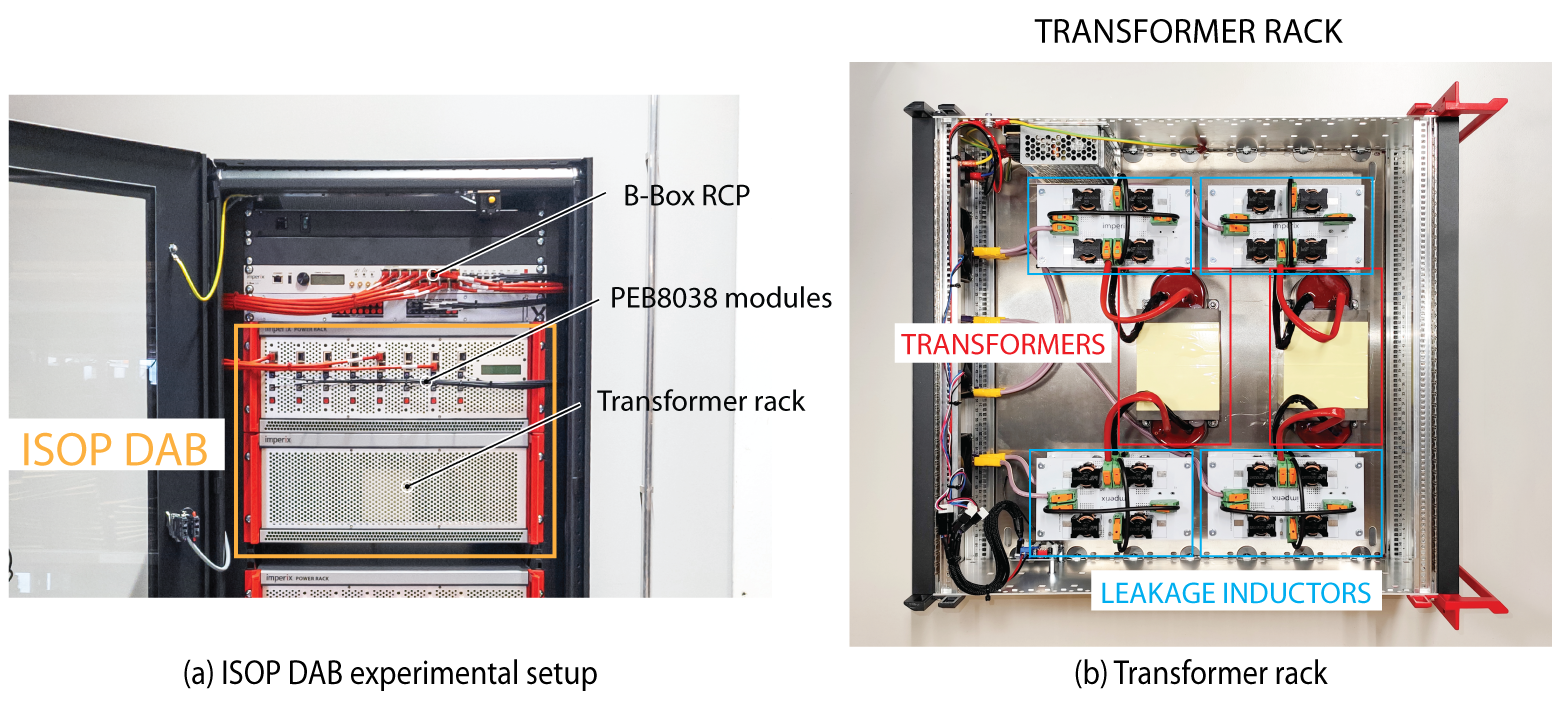
Experimental setup
The Matlab/Simulink model of the ISOP DAB system can be downloaded from the next link:
The DABs used for the experimental tests are built using the following components:
- A B-Box RCP controller.
- 2 full bridge converters per DAB, with each full bridge implemented using two imperix PEB8038 power modules.
- Two high-frequency transformers (SIRIO135822), one per DAB.
- Four leakage inductors (74437429203470) are connected in parallel at each transformer terminal to support higher peak currents, resulting in a total of 32 leakage inductors across the two DABs. Furthermore, to mitigate skin effect, litz wire inductors have been used. The total leakage inductance value has been selected according to the guidelines in TN119.
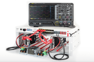
The ISO DAB setup and the inside of the transformer rack are depicted in Fig. 3.
The operating conditions are:
| Parameter | Value |
|---|---|
| Rated DAB power \(P\) | 10 kW |
| Input voltage \(V_{dc_s}\) | 400 V |
| Output voltage \(V_{dc_p}\) | 400 V |
| Transformer turn ratio \(n\) | 1 |
| Total leakage inductance \(L_{tot}\) | 47 µH |
| Magentization inductance | 0.7mH |
| Switching frequency \(f_{sw}\) | 20 kHz |
| Balancing gain \(K\) | 10 |
Experimental results
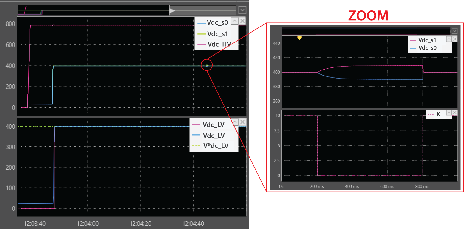
To experimentally validate the proposed control strategy for the ISOP DAB converters, a DC voltage source at 800 V was connected to the HV side, and a current source was used on the LV side. This configuration allows controllling the ISOP DAB output voltage, as using a voltage source on the LV side would have fixed the output voltage and limited the ability to regulate it during operation. The startup procedure for the DABs is based on the soft-start procedure explained in TN115.
In Fig. 4, the precharge and soft-start of the system can be observed. The first step involves precharging the input series capacitors. Following this, the soft-start process begins, during which the transformer is gradually magnetized by applying a slowly increasing current. This results in the progressive charging of the series-side DC bus capacitors. In the zoomed-in section of the figure, the effect of the balancing factor can be seen. For testing purposes, the balancing is disabled at t = 200 ms by setting \(K = 0\), leading to a balancing factor of \(k = 0.5\). This causes an equal distribution of the output currents between the DABs but leads to an imbalance in the input voltages. When the balancing control is reactivated, the input voltages return to a balanced state, demonstrating both the correct operation and the effectiveness of the proposed balancing strategy.
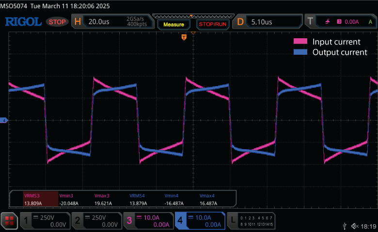
Finally, Fig. 5 and Fig. 6 show the voltages and the currents at the input and output of the transformer, respectively. As expected, the input and output voltages exhibit square waveforms. Regarding the currents, the slopes observed at the top and bottom of each period are due to the small difference between the input and output voltages. In a transformer where the magnetizing inductance is much larger than the leakage inductance, the magnetizing current can be neglected, resulting in nearly identical input and output currents. However, in this case, the ratio between the two inductances is approximately 15, making the magnetizing current non-negligible. Since the magnetizing current is the difference between the input and output currents, it leads to the observed difference in their slopes. Moreover, this magnetization current leads to higher losses, reducing the efficiency of the transformer.

Conclusions
In this note, a balancing method for a 2×2 ISOP DAB converter has been implemented. This method is simpler to implement compared to the commonly used three-loop control, as it relies on a feed-forward approach for power balancing and requires tuning only a single voltage controller. Furthermore, by incorporating the sign of the current in Eq. (1), the method supports bidirectional power flow. This means that in the case of an input-parallel-output-series (IPOS) DAB configuration, the same controller can be used, with the controlled voltage being the input voltage (still on the parallel side). However, if an ISOP DAB with more than two modules is used, the implemented controller is not easily scalable, and the use of the three-loop control described in [1, 2] is recommended.
Finally, regarding the transformer design, the results also highlight the importance of the ratio between the magnetizing inductance and the leakage inductance. If this ratio is not sufficiently large, a significant magnetizing current will flow, leading to lower efficiency and resulting in different waveforms for the input and output currents. To minimize this effect, the magnetizing inductance should be chosen to be much larger than the leakage inductance, thereby ensuring that the magnetizing current remains small and negligible.
References
[1] Chen, W., Ruan, X., Yan, H., & Tse, C. K, “DC/DC Conversion Systems Consisting of Multiple Converter Modules: Stability, Control, and Experimental Verifications”, in IEEE Transactions on Power Electronics, Vol. 24, 2009.
[2] C. Luo and S. Huang, “Novel Voltage Balancing Control Strategy for Dual-Active-Bridge Input-Series-Output-Parallel DC-DC Converters,” in IEEE Access, Vol. 8, 2020.
[3] Plexim, “Input-Series/Output-Parallel Dual Active Bridge.”, Online resource, Accessed June 2025.