Table of Contents
This technical note introduces the working principles of a single phase inverter. It presents a simple technique to generate an alternating current in an open-loop manner, using the imperix ACG SDK on Simulink or PLECS. This example can be used as an introduction to imperix tools as well as a reference model to develop more complete control schemas such as a single phase totem-pole PFC rectifier or a single phase PV inverter.
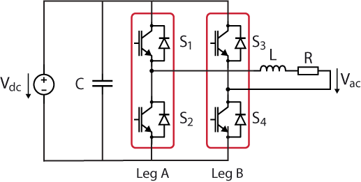
The considered circuit for the single phase inverter is represented below, where \(V_{dc}\) represents the DC voltage, L the output filter, R the load, and \(S_x\) the switching devices, which in this case are IGBTs.
Working principle
The main function of a single phase inverter is to generate an AC output waveform with minimal harmonic distortion from a DC input voltage. Single phase inverters are widely used in uninterruptible power supply (UPS) systems to deliver backup power during electrical outages. They convert DC power from batteries into AC power to ensure the continuous operation of critical equipment. Additionally, these inverters are commonly employed in renewable energy systems, such as solar inverters, to convert the DC output from solar panels into usable AC power.
As illustrated in the schematic of Fig. 1, it typically uses switching devices arranged in H-bridge configuration [1]. Alternatively, single phase inverter-based topologies, such as the totem-pole PFC, can also be found in the literature.
Modulation strategies
Different modulation strategies such as carrier based pulse width modulation (CB-PWM), space vector modulation or model predictive control can be used. On this technical note, the widely used sinusoidal PWM (SPWM) modulation strategy has been selected, which is based on a CB-PWM strategy with a sinusoidal reference. This modulation strategy calculates the commutation instants of the switching devices to obtain the desired AC output voltage, which is done by comparing the modulation signal (\(m_{ref}\)) with a carrier signal. Many variations have been proposed over the years with different carriers and reference waveforms [1]. In this technical note, the two-level and the three-level modulations are presented.
Two-level modulation
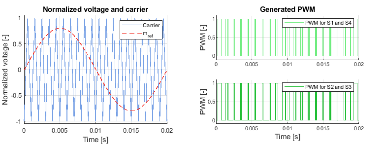
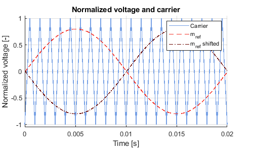
The two-level modulation, uses the same \(m_{ref}\) signal for both legs. The sinusoidal \(m_{ref}\) signal and the carrier used in this case, which happens to be triangular, are depicted in the figure below. As the same modulation signal is used for both legs, the switching devices S1-S4 and S2-S3 are turned on or turned off at the same time, generating an output of leg A equal and opposite to the output of leg B. When using this strategy, the line-to-line output voltage waveform can only have two different levels: \(+V_{dc}\) and \(-V_{dc}\).
Three-level modulation
With three-level modulation, both legs are modulated using the same triangular carrier but different modulation signals. The modulation reference used for leg B is the same as the one used for leg A but shifted 180º, as can be seen in the figure below. The line-to-line output voltage waveform switches between three different levels over a fundamental period: \(+V_{dc}\), 0 and \(-V_{dc}\).
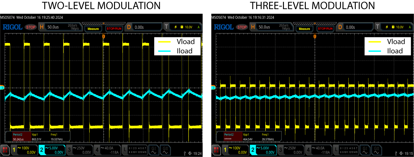
An interesting benefit of the three-level modulation is that the effective switching frequency is doubled when using this strategy, thus reducing the current ripple amplitude and the harmonic content when compared with the two-level switching strategy. This is illustrated in Fig. 7 and Fig. 8 of the experimental results.
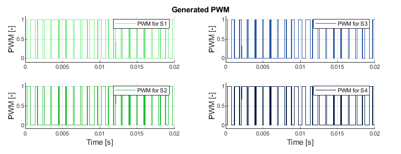
Implementation with imperix CB-PWM block
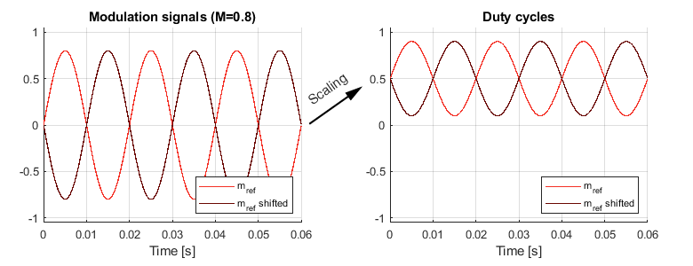
The Carrier-Based PWM block of the imperix library uses a PWM carrier varying between 0 and 1. Therefore, the modulation reference has to be normalized to the range [0, 1]. In the case where the original signals are in the range [-1,1], Eq. (1) can be applied for the normalization, where d represent the duty cycle and is the input to the imperix Carrier-Based PWM block:
$$(1) \quad d = \cfrac{m_{ref}}{2}+\frac{1}{2} \quad $$
In Fig. 4, the obtained duty cycles are represented when two sinusoidal signals shifted 180º are considered as \(m_{ref}\). Note that this normalization can be used for other \(m_{ref}\) signals.
Simulink and PLECS implementation
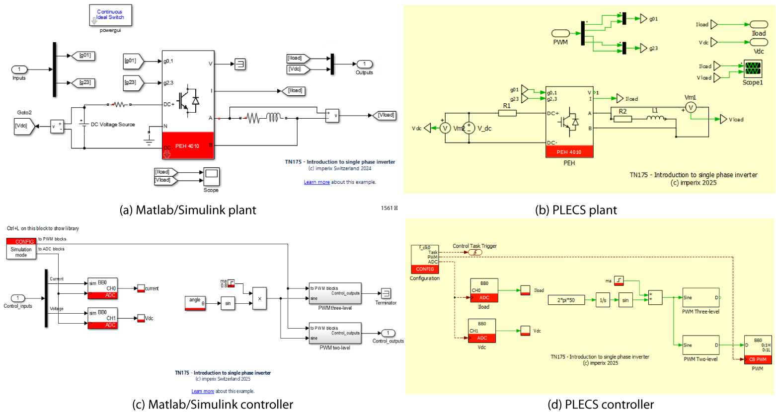
The open loop models for Simulink and PLECS of the full bridge single phase inverter connected to a RL load are given below. The \(m_{a}\) variable is the modulation index and represents the \(m_{ref}\) signal amplitude. To implement the converter model, the PEH4010 block from imperix power library has been used.
Simulink model
PLECS model
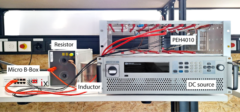
Hardware requirements
The following list describes the required hardware. It comprises imperix products as well as additional components commonly available in power electronic research laboratories:
- Imperix products
- 1x programmable controller (B-Box MICRO)
- 1x full-bridge module (PEH4010 or PEH2015)
- Control development tools for Simulink and PLECS (ACG SDK), with a valid license
- Additional hardware
- 1x inductor (2.2mH)
- 1x resistor (33Ω)
- A power supply
- Safety laboratory cables (banana)
Note that if the inductor and resistor values are different, the maximum output current limits have to be recalculated.
Experimental results
The two modulation strategies are tested using the setup shown below, where the converter is connected to an inductance and a load resistor. The schematic is illustrated in Fig. 1.
The tests are carried out for 300V DC voltage and a \(m_a = 0.9\). The voltage and current on the AC side obtained for both modulation strategies are shown in the next figure. As expected, when the two-level modulation is applied, a 2-level waveform is obtained at the output converter. On the other hand, with three-level modulation, the output voltage waveform has 3 levels.
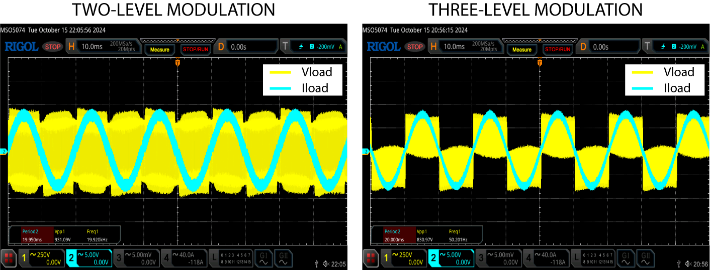
Additionally, when zooming in, it can be observed that the current ripple amplitude obtained using the two-level modulation is twice the ripple obtained with the three-level modulation. This is due to the effective switching frequency that is applied in each case. As observed, in the three-level modulation, the effective switching frequency is twice that of the two-level modulation, leading to a reduced current ripple amplitude and, therefore, to a reduced harmonic content.
Conclusions
In this technical note, two-level and three-level modulation techniques for a single phase inverter have been implemented. The experimental results show that the inverter switching frequency under three-level modulation is doubled. This provides better performance, as it results in a smaller current ripple and, consequently, lower harmonic content. Consequently, a smaller AC-side filter can be used without compromising performance, thereby reducing the size, weight, and cost of the inverter. The stress on the switches is also reduced with three-level modulation, as the voltage transitions are more gradual. Therefore, the use of this modulation technique is recommended for single phase inverters.
Going further with single phase inverter
For further reading about single phase applications, the following notes are recommended:
References
[1] Holmes, D.G. and Lipo, T.A. “Pulse Width Modulation for Power Converters: Principles and Practice”, IEEE Press Series on Power and Energy Systems, 2003.