Table of Contents
The TPI SV-PWM helper block is a wrapper that simplifies the use of the SV-PWM block with the all-in-one programmable inverter (TPI8032 22kW). Since the topology of the converter is fixed, the channel assignment and part of the modulators’ configuration are known beforehand.
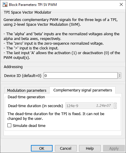
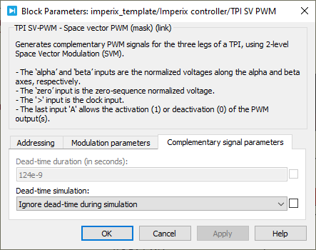
The topology of the converter and the connection of the PWM channels are shown below. To prevent short-circuiting the DC bus, the upper and lower leg switches always use pseudo-complementary signals with a fixed dead-time of 124 ns. This value was chosen as low as possible to minimize the distortion introduced by the dead-time.
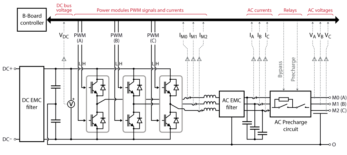
| PWM channel | PWM lane | Description |
| 0 | 0 | PWM High – Phase A (M0) |
| 1 | PWM Low – Phase A (M0) | |
| 1 | 2 | PWM High – Phase B (M1) |
| 3 | PWM Low – Phase B (M1) | |
| 2 | 4 | PWM High – Phase C (M2) |
| 5 | PWM Low – Phase C (M2) |
The TPI SV-PWM helper block is available starting from version 2024.2 of the SDK. The TPI8032 is required to use this driver.
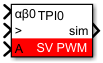
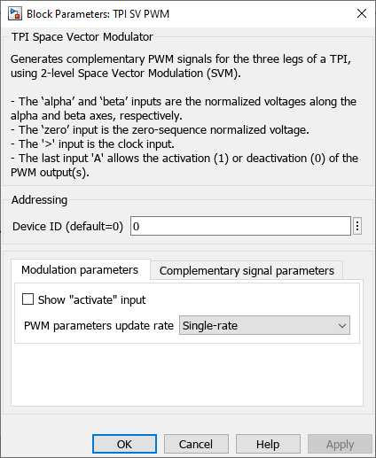
Simulink SV PWM helper block
Signal specification
- The input
αβ0is the normalized reference vector in the stationary reference frame (-1.15 to 1.15). - The input signal
>is the clock input and must be connected to the CONFIG block or to an independent CLK. - The input
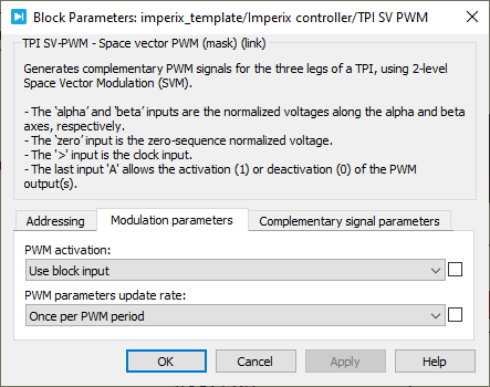
Aallows the activation (>0) or deactivation (<=0) of the PWM outputs. - The
simoutput is a vector corresponding to the six generated PWM signals (phase A high and low, phase B high and low, and phase C high and low). They are only used in simulation.
While each component of the normalized reference vector can be in the range [-1.15; 1.15], the norm of that vector must be in the range [0; 1.15]. The limitation of the norm is further explained in SVPWM vs SPWM modulation techniques (TN146). In addition, the page Space Vector Modulation (TN145) presents a way to take this limitation into account in a closed-loop control algorithm.
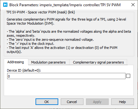
Parameters
Device IDselects which TPI to address when used in a multi-device configuration.Show "activate" inputmakes theAinput visible. If not checked, the TPI CB-PWM block is active by default.PWM parameters update rateselects when the duty-cycle parameter is applied.- Single-rate: it is applied at the end of the carrier period.
- Double-rate: it is applied twice per carrier period: when the carrier reaches its lowest point and when it reaches its highest point. (for TRIANGLE and INVTRIANGLE carriers only)
Simulate dead-timetoggles the option to simulate the effect of the dead-time.
PLECS SV PWM helper block
Signal specification
- The input
αβ0is the normalized reference vector in the stationary reference frame (-1.15 to 1.15). - The input signal
>is the clock input and must be connected to the CONFIG block or to an independent CLK. - The input
Aallows the activation (>0) or deactivation (<=0) of the PWM outputs. - The target output port (only visible at the atomic subsystem level) is a vector corresponding to the six generated PWM signals (phase A high and low, phase B high and low, and phase C high and low). They are only used in simulation.

While each component of the normalized reference vector can be in the range [-1.15; 1.15], the norm of that vector must be in the range [0; 1.15]. The limitation of the norm is further explained in SVPWM vs SPWM modulation techniques (TN146). In addition, the page Space Vector Modulation (TN145) presents a way to take this limitation into account in a closed-loop control algorithm.
Parameters
Device IDselects which TPI to address when used in a multi-device configuration.Show "activate" inputmakes theAinput visible. If not checked, the TPI CB-PWM block is active by default.PWM parameters update rateselects when the duty-cycle parameter is applied.- Single-rate: it is applied at the end of the carrier period.
- Double-rate: it is applied twice per carrier period: when the carrier reaches its lowest point and when it reaches its highest point. (for TRIANGLE and INVTRIANGLE carriers only)
Simulate dead-timetoggles the option to simulate the effect of the dead-time.
C++ functions
There are no C++ helper functions for the TPI. Please refer to the generic SV-PWM functions.