Table of Contents
Debugging an FPGA design can be difficult without clear visibility into the high-speed logic fabric, where signals change at nanosecond scales. Xilinx Integrated Logic Analyzer (ILA) provides that visibility by acting as an embedded oscilloscope inside the FPGA. It captures internal signals in real time and stores them in dedicated Block RAM (BRAM) for cycle-accurate observation.
To make the ILA practical to use to FPGA sandbox users, imperix supports the Xilinx Virtual Cable (XVC) protocol. This Ethernet-based protocol acts like a JTAG cable and provides a means to connect to ILAs without opening the enclosure to attach a physical debugger.
The latest version of the IP is available on the download page and PN174 provides a step-by-step guide on upgrading an existing FPGA design.
Enabling the debug interface
Before adding ILA cores to a design, the debug infrastructure must be enabled in the imperix firmware IP. This allows Vivado to communicate with the debug cores over the network via the XVC protocol.
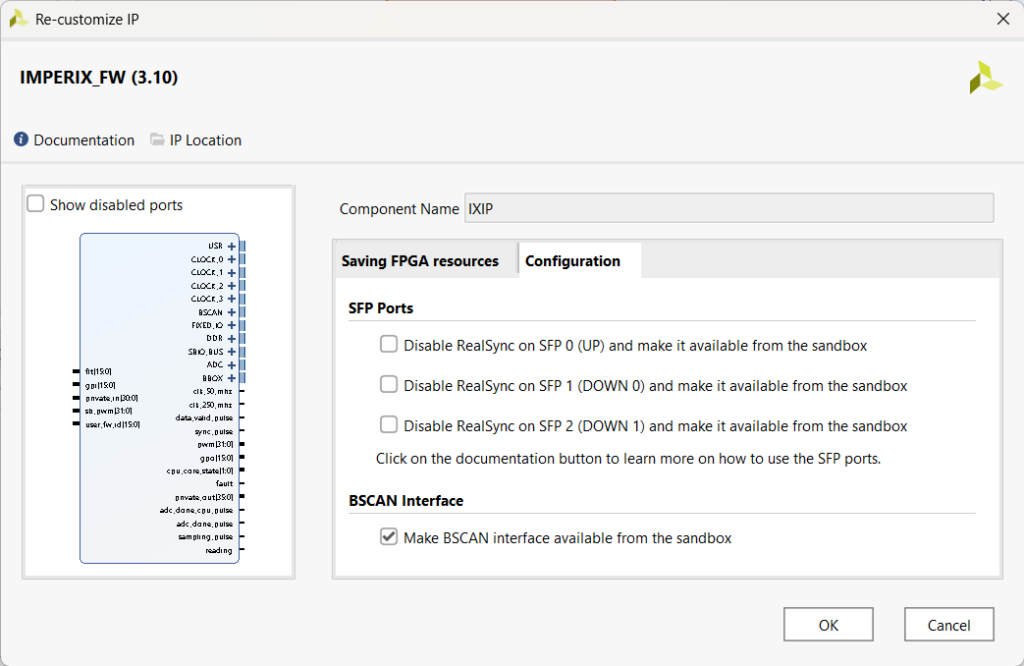
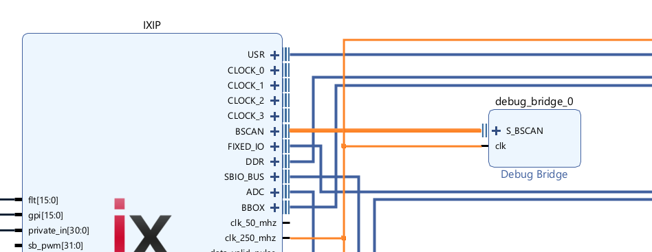
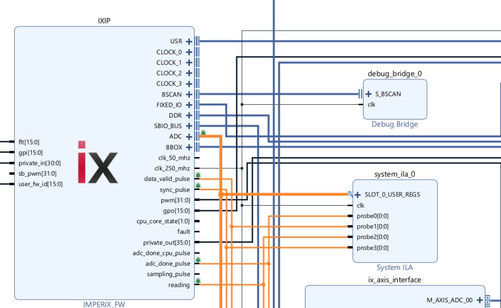
- Enable BSCAN in the imperix firmware IP. The BSCAN (Boundary Scan) interface is the virtual port that provides access to the FPGA debug chain.
- Double-click the IMPERIX_FW IP in the block design to open the configuration dialog.
- Navigate to the Configuration tab.
- Check the Make BSCAN interface available from the sandbox and click OK. This exposes a BSCAN port on the IP block.
- Add and connect the Debug Bridge IP. The Debug Bridge acts as a switch, routing commands from the CPU to all connected debug cores.
- Right-click in the block design and select Add IP.
- Search for Debug Bridge and add it to the design.
- Double-click the Debug Bridge to configure it and ensure the Bridge Type is set to From BSCAN to DebugHub.
- Connect
S_BSCANto theBSCANport of theIMPERIX_FWand connectclktoclk_250_mhz.
Adding signals to the ILA
While the remote XVC network architecture is specific to the controller environment, instantiating and operating the ILA cores relies entirely on standard Xilinx Vivado workflows. The following sections summarize these standard procedures for convenience.
- In the block design, right-click on the signals/wires to be observed
- Select Debug from the context menu
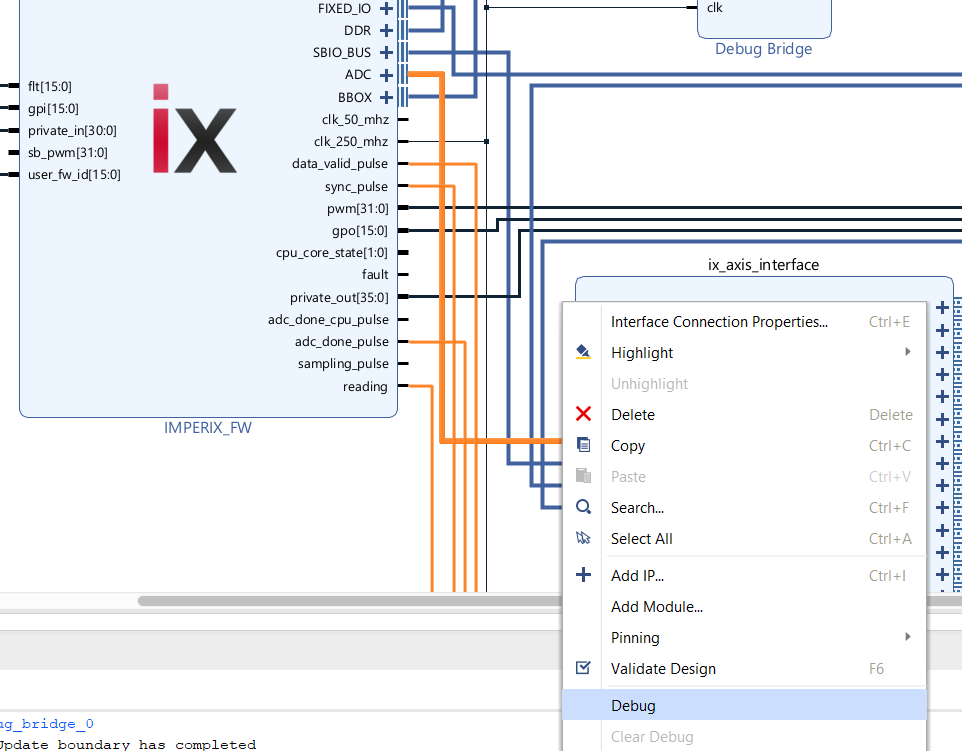
- A debug marker (small bug icon) appears on the signal, and a green banner appears at the top: “Designer Assistance available. Run Connection Automation”
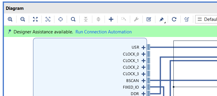
- Click Run Connection Automation
- In the dialog, configure the ILA options:
- Probe Type: Select “Data and Trigger” to use the signal for both capture and triggering
- Source Clock: Select the clock for the signal’s domain (typically
/IXIP/clk_250_mhz) - System ILA: Leave as “Auto” to let Vivado create a new ILA
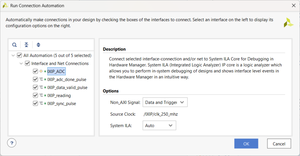
- Click OK. Vivado automatically creates a System ILA and connects everything.
Configuring the ILA
After creating the System ILA, double-click the block to open the configuration dialog. Depending on whether individual wires or full AXI interfaces are being monitored, the dialog displays up to three main tabs:
1. General Options tab
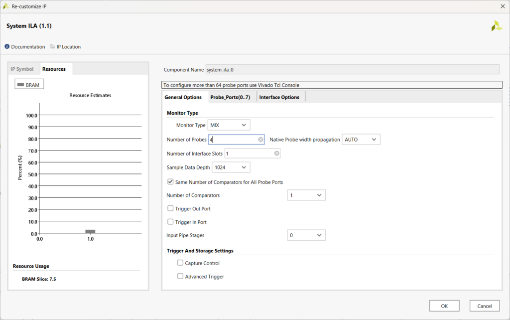
- Sample Data Depth: Sets the number of samples to capture. Increasing this value extends the capture window but consumes more Block RAM.
- Number of Probes: Total number of individual signal ports. This value can be increased to manually add probes beyond those created by automation.
- Number of Comparators: Sets the comparison units per probe for trigger conditions. One is usually sufficient unless complex logic is required.
2. Probe_Ports tab
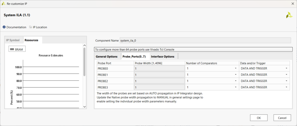
- Probe Width: Defined in bits. With “Native Probe width propagation” set to AUTO, this matches the connected signal automatically.
- Data and/or Trigger: Sets whether a probe is used for data capture, triggering, or both.
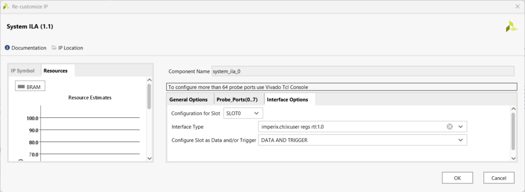
3. Interface Options tab This tab appears when full interfaces (such as AXI4-Stream) are connected to the ILA. It enables the configuration of specific slots and signals within the interface for use in triggering or data storage.
The Resources panel on the left provides real-time estimates of Block RAM usage, helping to balance capture depth against available hardware resources.
Managing clocks and capture windows
The ILA must be clocked by the same source driving the signals under observation; using a different clock will result in unstable or incorrect data. For most sandbox designs, connect the ILA clock input to clk_250_mhz.
The duration of the capture window is determined by the sample depth and the clock frequency. At a standard 250 MHz frequency, the capture times are as follows:
| Sample Depth | Capture Time at 250 MHz | Approximate BRAM Usage |
| 1024 | 4.1 µs | 1 BRAM per 36-bit probe |
| 2048 | 8.2 µs | 2 BRAM per 36-bit probe |
| 4096 | 16.4 µs | 4 BRAM per 36-bit probe |
Operating the ILA in Vivado
Once the bitstream is generated and loaded into the controller using Cockpit, signals can be accessed through the Vivado Hardware Manager.
Establishing the XVC connection
- Open Hardware Manager in Vivado (Flow Navigator → Program and Debug → Open Hardware Manager)
- Click Open Target → Open New Target
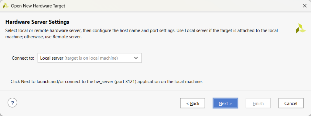
- In the Hardware Server Settings, select Local server and click Next
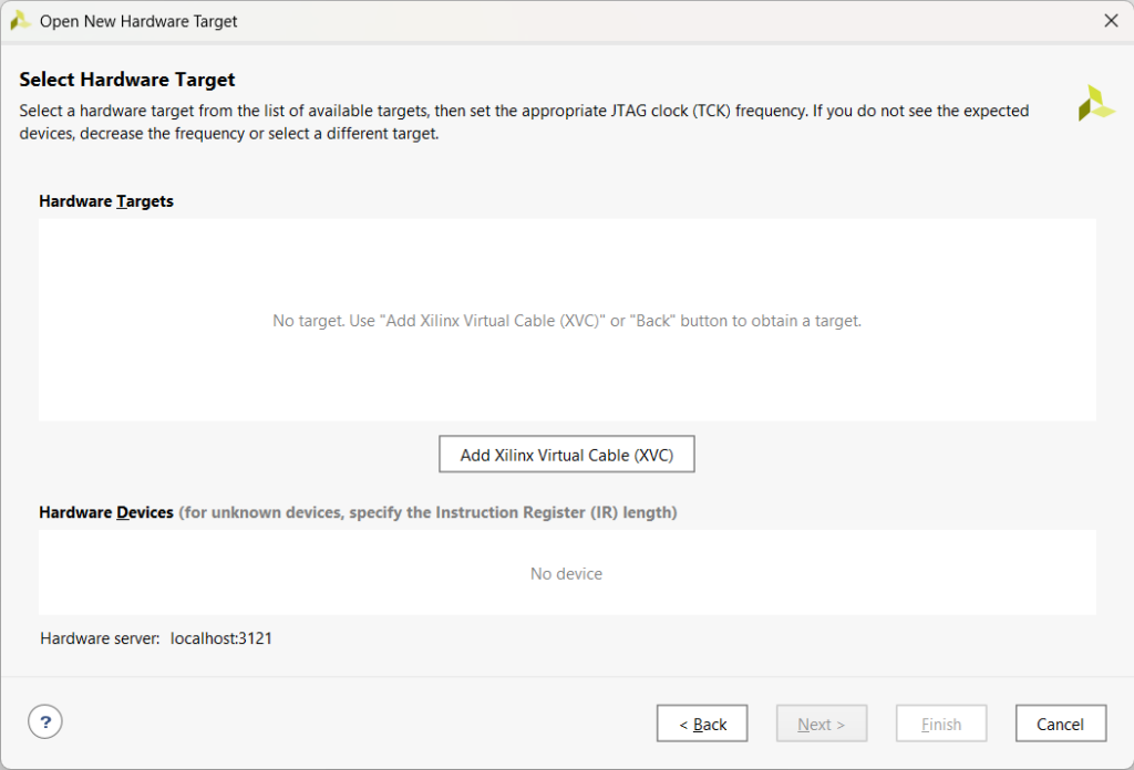
- In the Select Hardware Target screen, click Add Xilinx Virtual Cable (XVC)
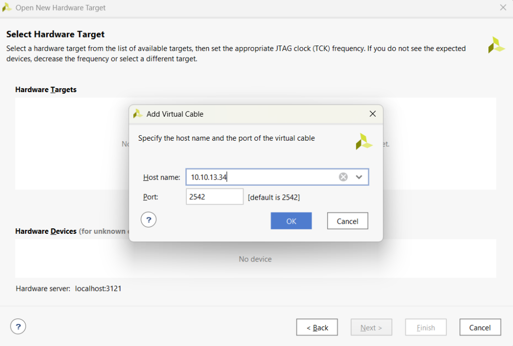
- Enter the IP address of the imperix device and port 2542 (default XVC port), then click OK
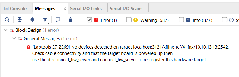
- An error message similar to this one can appear. This error can be safely ignored and seems to be a bug on Vivado’s side.
- Click Next and Finish to complete the connection. Vivado will detect the debug bridge and ILA core.
Loading the probes file
After connecting, the ILA appears but shows “No probes exist”. The probes file that was generated during bitstream implementation must be loaded.
- In the Hardware panel, click on debug_bridge_0
- In the Hardware Device Properties panel below, locate the Probes file field
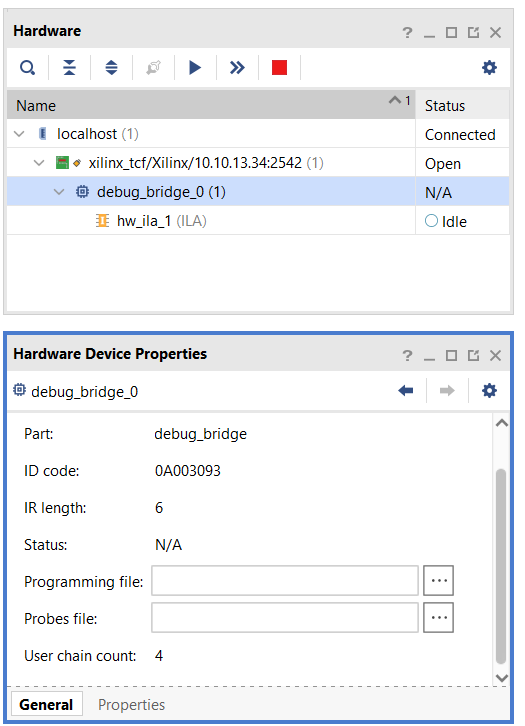
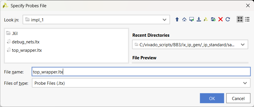
- Click the … button and navigate to the Vivado project folder
vivado/<PROJECT_NAME>/<PROJECT_NAME>.runs/impl_1/ - Select the top_wrapper.ltx file (or similar
.ltxfile) and click OK
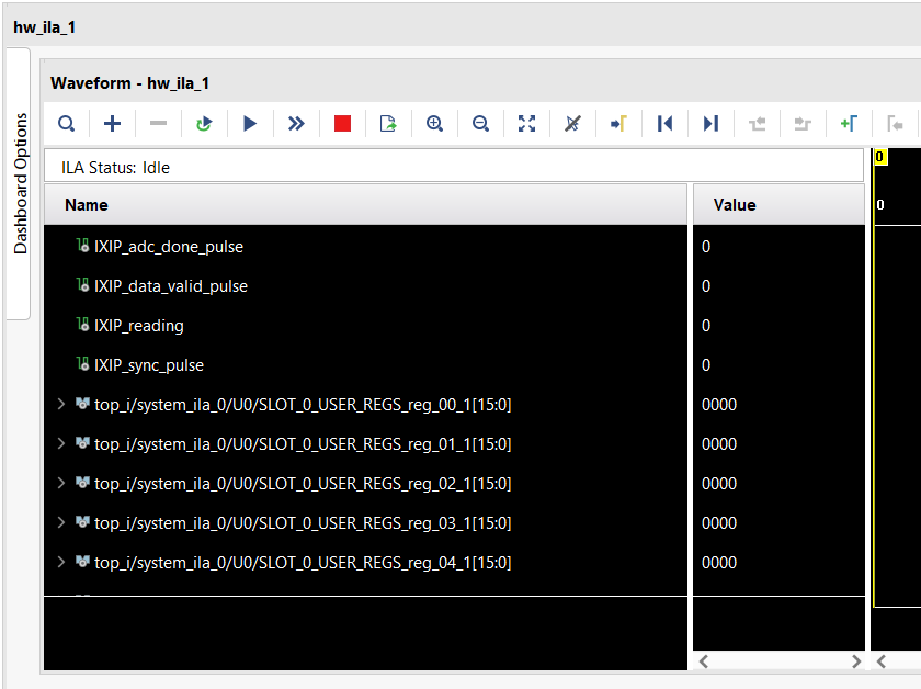
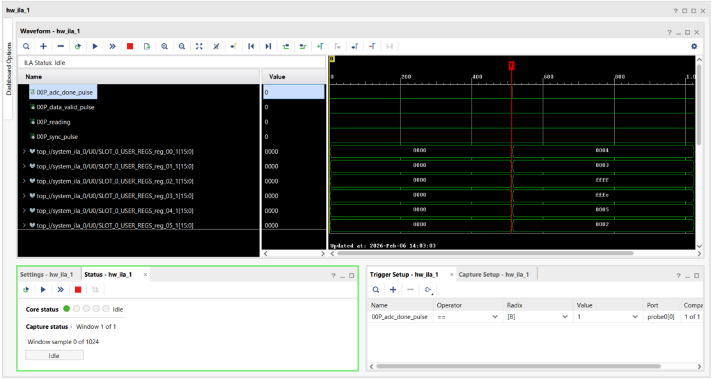
- The probes are now loaded and visible in the waveform viewer
Operating the ILA
Immediate trigger: Click the Run Trigger Immediate button (>>) to capture data immediately without waiting for a trigger condition.
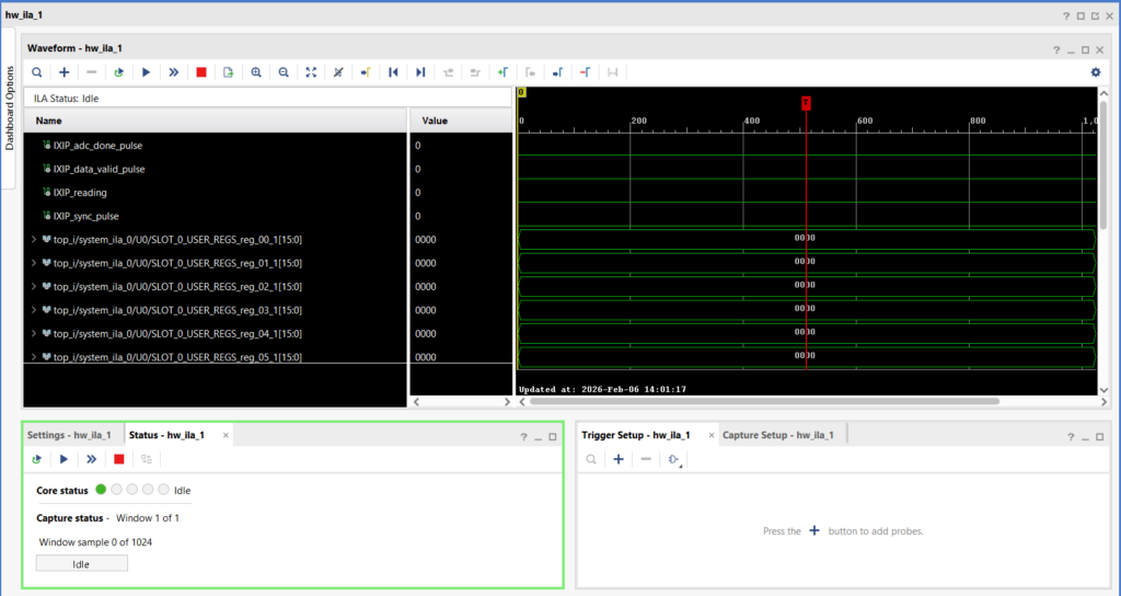
Conditional trigger:
- In the Trigger Setup window, add the probes to be used as trigger sources
- Set the trigger condition (e.g.,
probe0 == 1orprobe1 rising edge) - Click “Run Trigger” (▶ with T) to arm the ILA and wait for the condition
To go further
The example at the end of PN127 demonstrates how an ILA can be used to verify a PWM modulator implemented in the FPGA sandbox.
The latest section of the FPGA-based control of a grid-tied inverter example shows how to use an AXI4-Stream Broadcaster to split a stream and route it to the CPU. This allows connecting the result to a probe and observe it from Cockpit, which is sometimes more convenient than using an ILA.