
Table of Contents
Imperix B-Box controllers, as well as the B-Board PRO, feature dedicated pins that connect directly from/to the FPGA, without any intermediary circuitry. In total, 36 bidirectional I/Os are available, regrouped under the designation USR pins. Being directly connected to the FPGA, the USR bus guarantees maximum performance and flexibility for users, enabling baud rates over 200 Mbps.
Customizing the FPGA firmware involves instantiating the imperix firmware IP within AMD/Xilinx Vivado to edit the surrounding programmable logic, known as the sandbox. Step-by-step instructions for starting a new project from the provided template are available in the getting started guide.
Physical location of the USR pins
The following table details the physical location of USR pins:
| Controller | Location of the USR pins | Related datasheet/page | |||
|---|---|---|---|---|---|
| B-Box 4 | VHDCI connector B (*) | B-Box 4 datasheet | |||
| B-Box 3 (RCP) | VHDCI connector B (*) | B-Box RCP datasheet | |||
| B-Box Micro | VHDCI connector (*) | B-Box Micro datasheet | |||
| B-Board PRO on its Eval-Board | 36-pin 2.54 mm header | Carrier Board description page | |||
| B-Board PRO | JX2 connector | B-Board PRO datasheet | |||
| Programmable inverter (TPI8032) | Not available. | ||||
(*) Accessible via a breakout board such as the VHDCI breakout board.
Using the USR pins
There are two specific cases where the USR pins are reserved by imperix and are unavailable for custom applications:
- In the TPI8032, these pins are used to retrieve extra measurements and fault flags.
- In a B-Box, when using a motor interface, the signals from/to the interface are carried over USR pins.
If neither of these conditions applies, the default USR interface port can be safely deleted. The pins then become free to use for any custom purpose within the FPGA sandbox. For that, four steps are required:
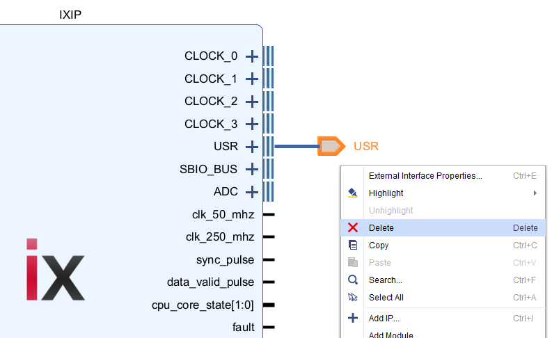
1. Delete the existing USR interface port
- Right-click on the existing USR interface.
- Click Delete.
2. Create new interface ports
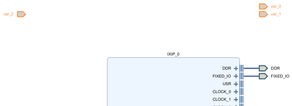
- Right-click, then Create Port…
- Give it a name, select a direction, and click OK.
3. Edit the constraints
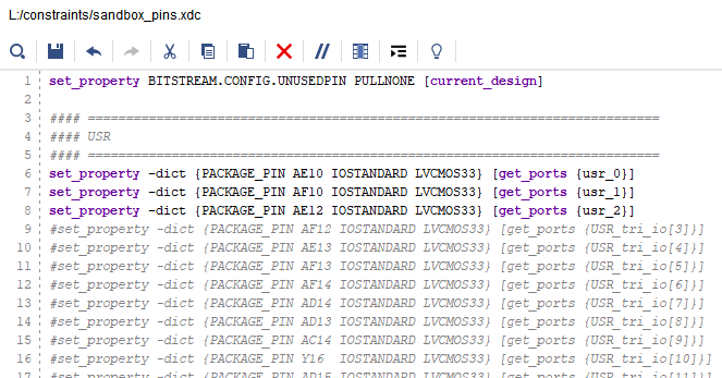
The constraints\sandbox_pins.xdc must be edited accordingly. As shown below, we recommend commenting (#) the unused pins to avoid generating unnecessary warnings in Vivado. For more information on constraints in Xilinx FPGA, please refer to the Using Constraints in Vivado Design Suite user guide.
4. Update the block design wrapper
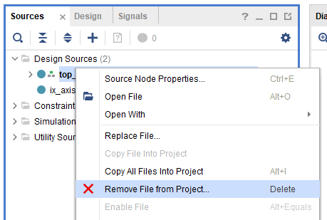
Whenever top-level ports are modified, the block design wrapper must be updated to reflect the changes. The recommended procedure is the following:
- Remove the existing wrapper by right-clicking on top_wrapper and select Remove File from Project.
- Check the Also delete the project file from disk option, then OK.
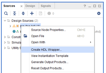
- In the Design sources of the Sources panel on the left, right-click on top (top.bd) and select Create HDL wrapper.
- Check Copy generated wrapper to allow user edits. Press OK.
To go further
The following application notes illustrate practical uses of the 3.3V USR pins for communicating with external peripherals:
 By Shu Wang • June 10, 2021 • TN140
 By Jules Perrin • April 16, 2026 • PN129