Table of Contents
Imperix controllers offer a simple way to arrange user-defined data transfers between the CPU and the FPGA using dedicated read and write registers. Data is automatically retrieved before the execution of the user control task and automatically written afterward, similar to other I/O resources. These registers are designated as SBI and SBO, respectively standing for “Input from Sandbox” and “Output to Sandbox”.
From the perspective of the user code, the SBI/SBO registers are handled very similarly to the GPI and GPO resources, except that they provide access from/to signals inside the FPGA sandbox rather than physical I/Os. At the hardware level, data exchanges with these registers are handled in the same way as with other I/O peripherals, as explained in PN253.
Ultimately, when working with the ACG SDK, the SBI/SBO registers enable users to easily read from (or write to) the FPGA using Simulink or PLECS blocks. The same mechanism also applies to users of the CPP SDK via dedicated routines.
Customizing the FPGA firmware involves instantiating the imperix firmware IP within Xilinx Vivado to edit the surrounding programmable logic, known as the sandbox. For step-by-step instructions on creating the required FPGA sandbox template, refer to the getting started guide.
SBIO bus
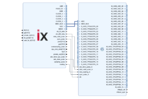
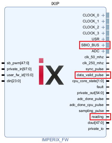
From the perspective of an FPGA sandbox user, the CPU communicates with the FPGA via the SBIO_BUS (SandBox IO bus), which is directly available on the imperix firmware IP. This proprietary bus is a 16-bit memory-mapped bus, which enables the CPU to read and write up to 1024 FPGA registers.
The reading and data_valid_pulse Signals can be used to synchronize user logic with the CPU’s read and write cycles. However, direct interaction with these signals is rarely necessary, as the SBIO helper modules, described in the following section, are available.
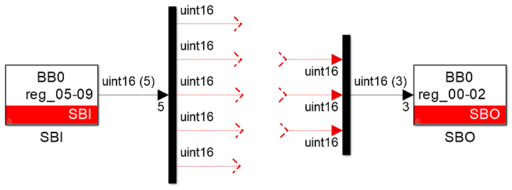
From the perspective of the Simulink/PLECS control model (or user code), the user interacts with the SBIO bus using the following blocks:
- SBI blocks to read FPGA registers before the execution of the CPU task.
- SBO blocks to write FPGA registers after the execution of the CPU task.
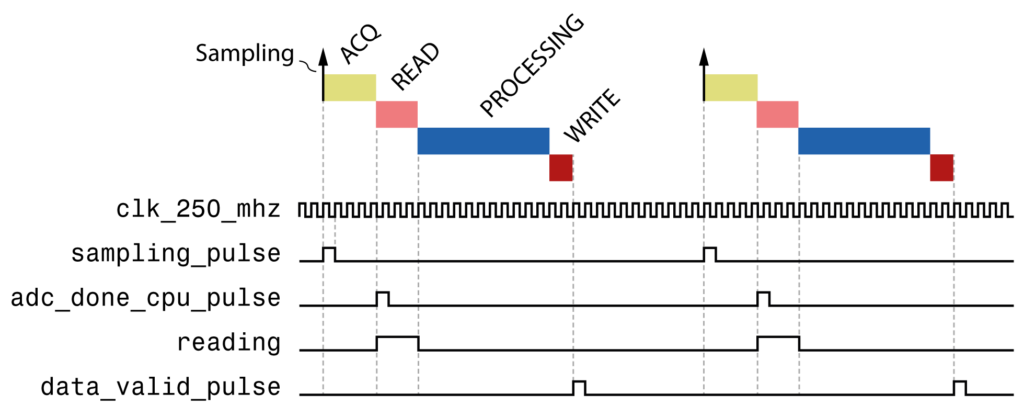
The image below illustrates the typical control execution process, which is described in more detail in the imperix firmware IP product guide. Before and after the CPU-based processing of the user code, two phases should be identified, during which the data exchanges take place:
- The Read phase is indicated by the assertion of the
readingsignal. During that time, SBI registers are read and cached in the CPU buffer, making them available to the user application. - At the end of the processing phase, SBO values are written to the FPGA. The end of the Write phase is indicated by the assertion of the
data_valid_pulsesignal.
SBIO helper modules
The following SBIO helper modules are included in the imperix source files to abstract away the complexity of the SBIO bus.
SBIO registers
The sbio_registers and sbio_256_registers modules provide 64 and 256 16-bit registers, respectively.
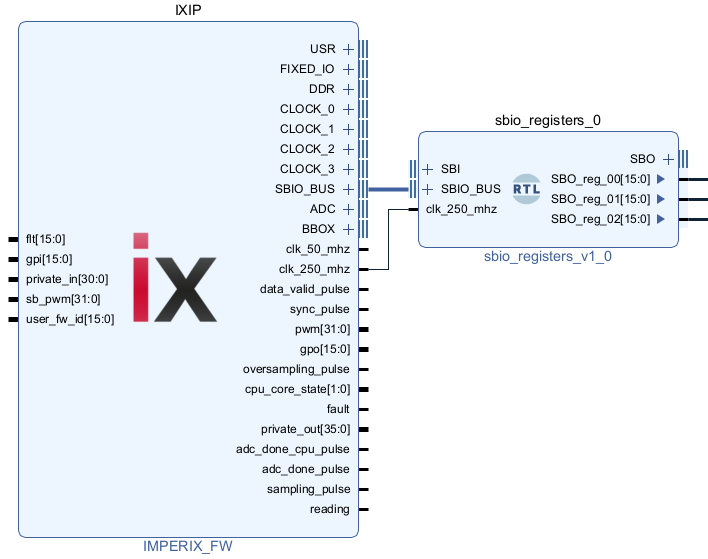
sbio_registers moduleSBIO interconnect
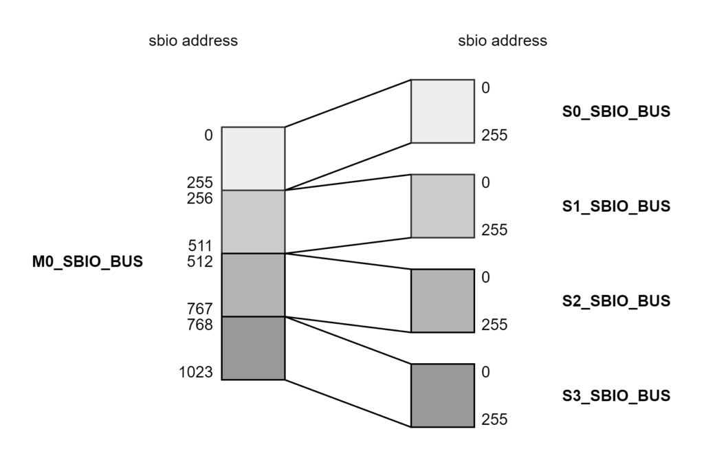
The sbio_interconnect divides the full 1024-address range of the SBIO bus into four 256-address ranges, allowing multiple SBIO modules to be connected.
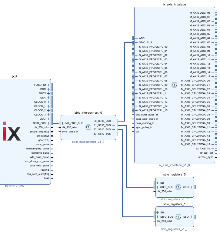
sbio_interconnect used to connect multiple SBIO modules to the SBIO_BUSThe address mapping of the SBIO interconnect is shown below; it divides the SBIO addressable range into 4 smaller areas.
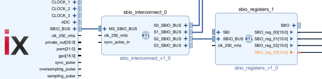
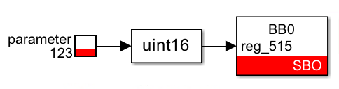
As an example, writing to SBO_reg_03 of an sbio_register block connected to S2_SBIO_BUS requires an SBO block addressed to register 512 + 3 = 515.
AXI4-Stream interface
The AXI4-Stream interface provided with the sandbox template allows exchanging 32-bit data between the CPU and FPGA using the M_AXIS_CPU2FPGA and S_AXIS_FPGA2CPU interfaces.
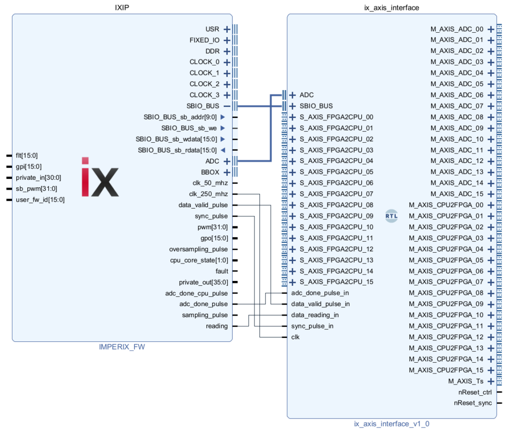
The AXI4-Stream interface was designed specifically to facilitate the implementation of control algorithms in FPGAs, such as the high-speed current control described in TN147. The interface is designed for algorithms that share the following characteristics:
- The control algorithm is fully implemented in the FPGA.
- The control algorithm is executed at the ADC sampling rate (SCLK rate), which may be faster than the CPU rate (postscaler > 1).
- The control algorithm operates with 32-bit floating-point data.
- The CPU model is used to write slow-varying signals such as configuration parameters (Kp, Ki, etc.) and slow-varying references, or serves for monitoring/debugging purposes.
To facilitate the design of such algorithms, the following design choices were made:
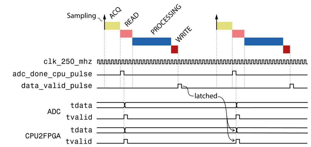
- The M_AXIS_ADC and M_AXIS_CPU2FPGA interfaces output data at the same time, synchronized to the
adc_done_pulse. The consequence is that CPU2FPGA signals are delayed to the end of the next acquisition phase.
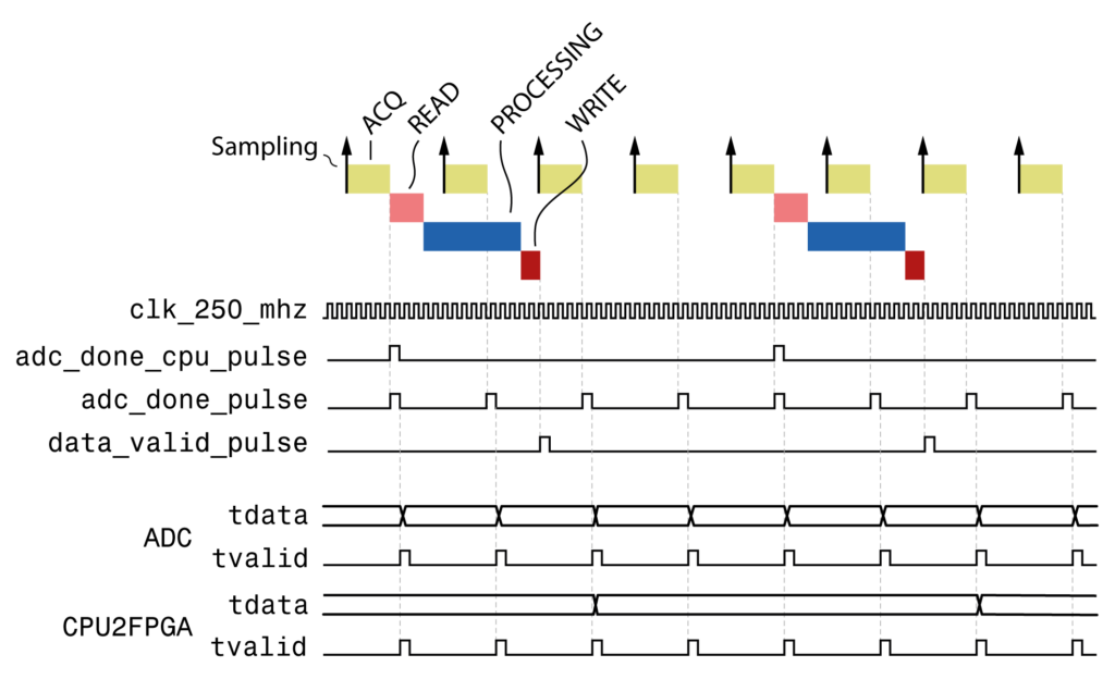
- The M_AXIS_ADC and M_AXIS_CPU2FPGA interfaces output data at the same rate. That means that when the CPU execution rate is slower than the sampling clock (postscaler > 1), the same CPU2FPGA values are outputted multiple times.
Address mapping of the AXI4-Stream interface
The mapping between the 16-bit SBIO registers and the 32-bit AXI4-Stream interfaces is the following:
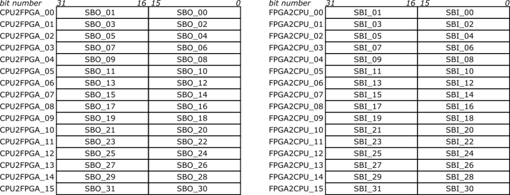
These registers are typically used to exchange floating-point values with the CPU. Ready-to-use helper functions for Simulink and PLECS are provided in the next section.
Exchanging floats signals
Algorithms typically operate using 32-bit floating-point values. The Simulink and PLECS templates provided below provide ready-to-use scripts to concatenate or decompose the 16-bit values and interpret the result as a floating-point variable.
Simulink model

In Simulink, the following MATLAB functions are used:
sbi2single
function y = sbi2single(u1,u2)
  y = single(0); % fix simulink bug: force compiled size of output
y = typecast([uint16(u1) uint16(u2)], 'single');single2sbo
function [y1,y2] = single2sbo(u)
  temp = typecast(single(u),'uint16');
  y1 = temp(1);
y2 = temp(2);PLECS model

The PLECS C-Script functions are provided below:
sbi2single
float y1 = InputSignal(0,0);
float y2 = InputSignal(0,1);

union { unsigned int i; float f; } conv;
conv.i = ((unsigned short)y2 << 16) | (unsigned short)y1;

OutputSignal(0,0) = conv.f;single2sbo
union { unsigned int i; float f; } conv;

conv.f = InputSignal(0,0);

OutputSignal(0,0) = (unsigned short)(conv.i & 0xFFFF);
OutputSignal(0,1) = (unsigned short)(conv.i >> 16);Example using the AXI4-Stream interface
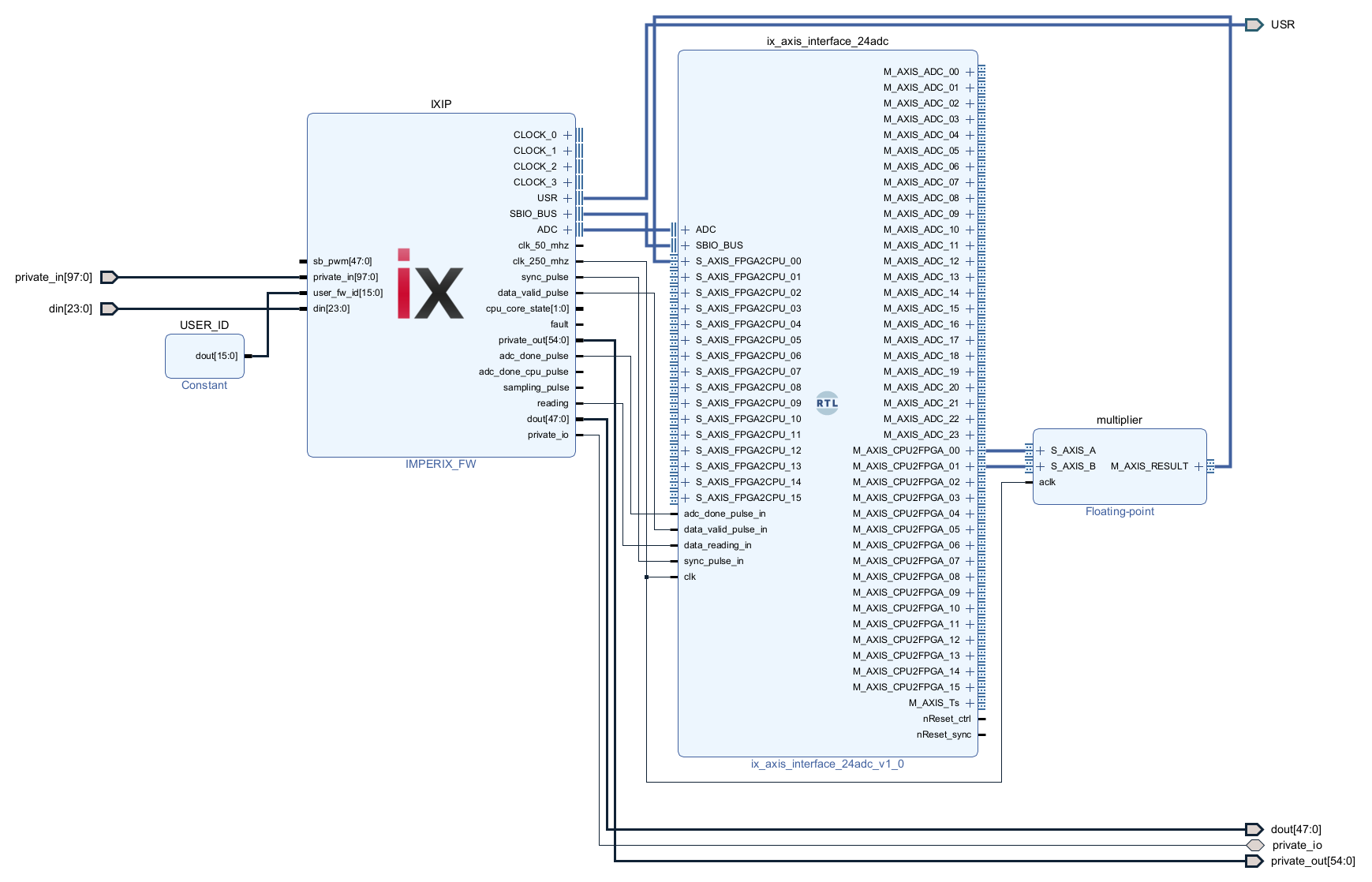
This step-by-step example implements the FPGA design shown below, which:
- Receives two floating-point values from the user application (
CPU2FPGA_00andCPU2FPGA_01). - Multiplies the two values together using a Xilinx Floating-Point IP.
- Sends the result back to the user application running in the CPU (
FPGA2CPU_00).
1. Start from the sandbox template
Create the Vivado sandbox template following the procedure detailed in the Getting started guide for FPGA programming.
2. Add a multiplier
To add an AXI4-Stream IP that multiplies two floating-point values:
- Right-click somewhere in the block design, select Add IP, and search for Floating-point. Press Enter.
- In the Block Properties panel, rename the block to multiplier.
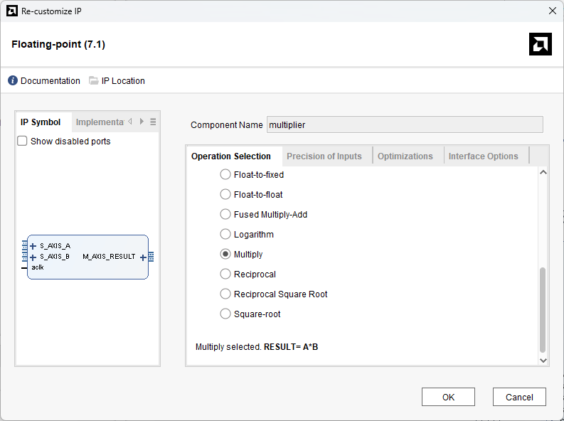
- Double-click on the IP to open the configuration panel. In the Operation Selection tab, select Multiply for the operation. Other parameters can be left in their default configuration.
3. Connect the multiplier
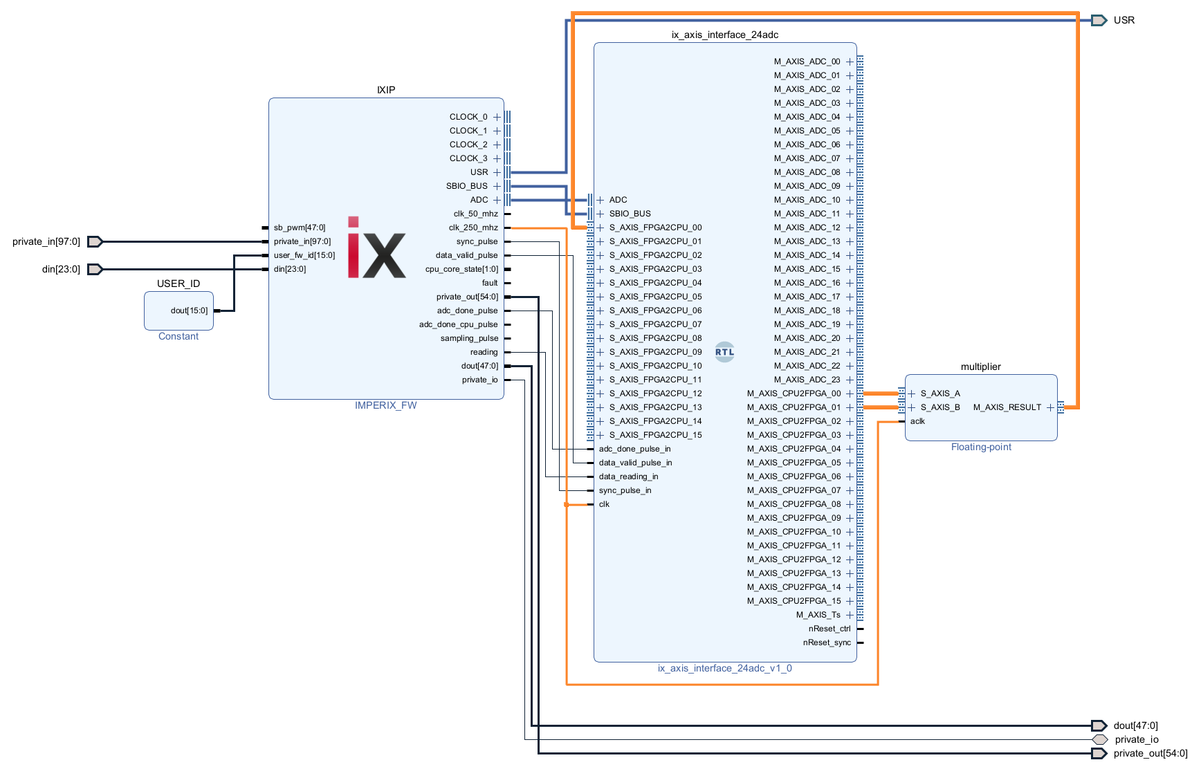
The design can be finalized by applying the following connections between the AXI4-Stream interface and the multiplier:
- M_AXIS_CPU2FPGA_00 to S_AXIS_A
- M_AXIS_CPU2FPGA_01 to S_AXIS_B
- M_AXIS_RESULT to S_AXIS_FPGA2CPU_00
The aclk signal of the multiplier must be connected to the clk_250_mhz clock.
4. Save, build, and load the design
- Save the design, then click Generate bitstream in the left sidebar.
- Load the bitstream onto the controller via Cockpit.
Experimental validation
The FPGA design is tested using the CPU model provided below. It contains two tunable parameters for the two operands, which are transmitted to the FPGA via SBO blocks, and the result is received from the FPGA via an SBI block. The sbi2single and single2sbo conversions are described in the section above about exchanging floats.
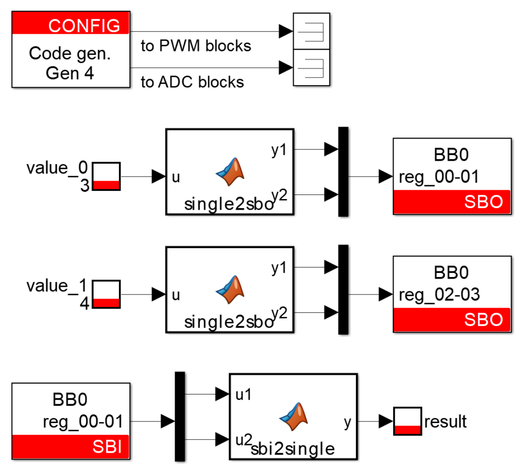
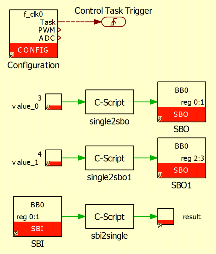
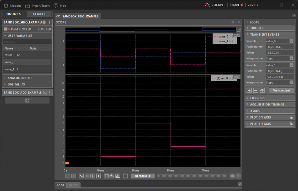
The expected results are shown in the figure below, obtained by varying both operands using Cockpit’s built-in transient generator.
Going further
TN147 uses the AXI4-Stream interface for the CPU model to interact with the current control implemented in the FPGA. The CPU2FPGA interfaces are used to write configuration signals (Kp, Ki, etc.) and slow-varying references (Iref), while the FPGA2CPU interfaces are dedicated to monitoring and debugging.
In PN127, a PWM modulator is implemented on an FPGA, and the duty cycle is provided by the CPU model. To avoid the additional delay introduced by the AXI4-Stream interface, the sbio_register helper is used instead. Two SBO registers are concatenated to form a 32-bit floating-point value.
 By François Ledent • April 16, 2026 • PN127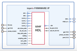
 By Benoît Steinmann • March 26, 2021 • PN116