Table of Contents
Imperix provides direct access to ADC measurements within the FPGA which allows for reduced delay between the sampling and the processing, but also helps supporting higher sampling frequencies.
In imperix devices, the ADC measurements are performed by the data acquisition stage, which is shared by both the CPU and FPGA control paths. From the sandbox, the FPGA development environment for imperix controllers, users have direct access to the ADC measurements from the acquisition module.
After a brief introduction to the data acquisition architecture, this page explains how to access the ADC measurements from the sandbox as registers or as AXI4-Stream interfaces. A practical example finally illustrates how to retrieve ADC samples from the sandbox, compute and apply the appropriate scaling gain to convert the raw data into physical quantities and apply it.
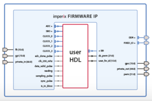
Customizing the FPGA firmware involves instantiating the imperix firmware IP within Xilinx Vivado to edit the surrounding programmable logic, known as the sandbox. For step-by-step instructions on creating the required FPGA sandbox template, refer to the getting started guide.
Data acquisition architecture
The general architecture of imperix controllers is documented in the imperix IP product guide. Below is a detailed view of the data acquisition module, which pilots the ADC chips and make the analog input measurement available to the user-programmable FPGA area via the following interfaces:
- ADC interface, which returns raw 16-bit measurements;
- ADC_FLOAT interface (B-Box 4 only), which returns the physical (post-rescaling) values in a 32-bit floating-point format.
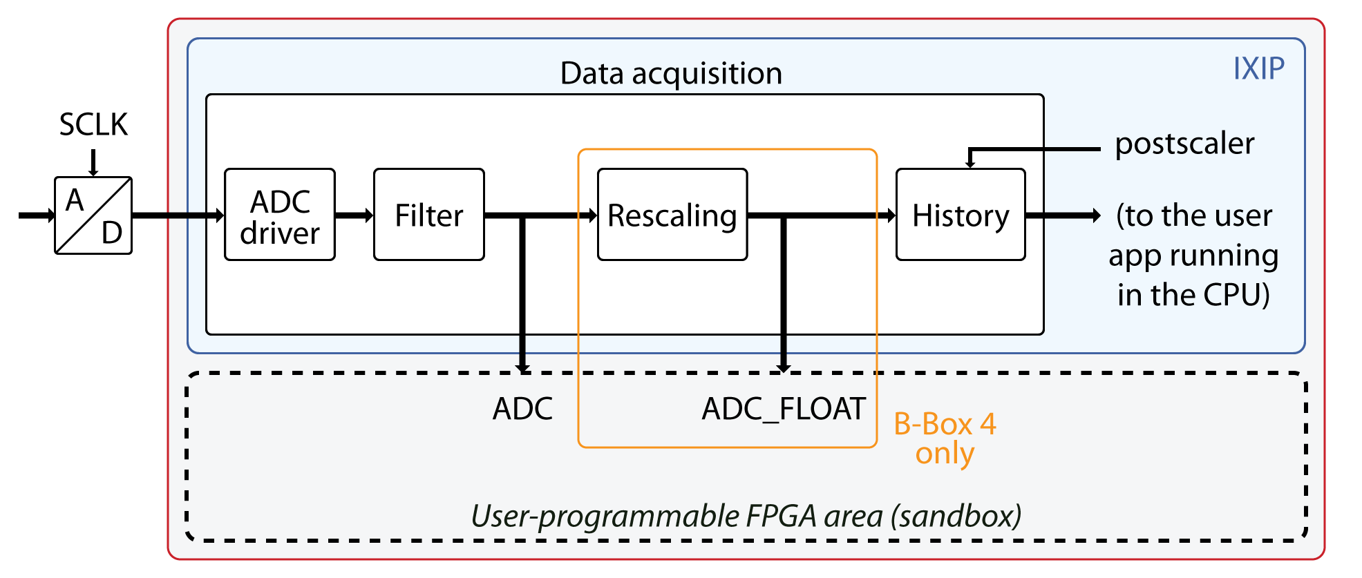
The data acquisition module is composed of the following stages:
- The ADC driver retrieves measurements from the ADC chip.
- The filter implements the synchronous sampling or averaging (all devices), or low-pass filter (B-Box 4 only), which can be enabled from the ADC block. The filtering techniques are detailed in PN158.
- The rescaling module (B-Box 4 only) converts the raw ADC data into physical values using the sensitivity and offset values specified in the ADC block. On other devices, this conversion is performed within the CPU.
- The history module allows to retrieve older samples from the ADC block, which is used typically when the CPU interrupt frequency is set to be slower than the FPGA sampling frequency (SCLK) using the postscaler.
This scenario is further documented in the Handling different execution rates of PN116.
Accessing ADC samples from the FPGA sandbox
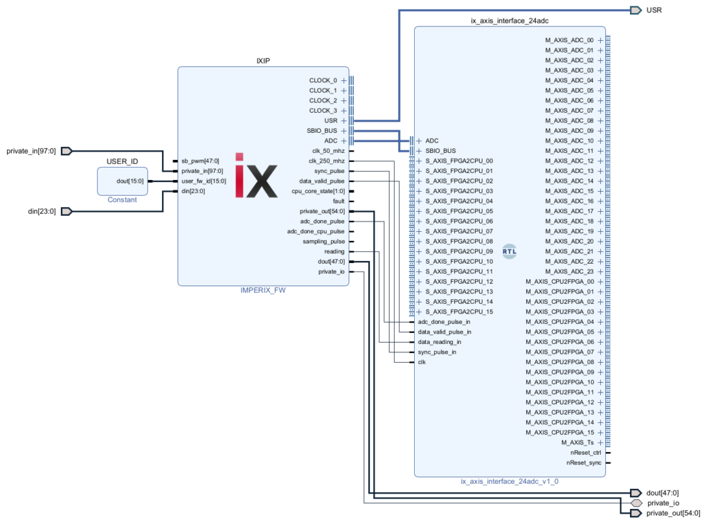
In the FPGA sandbox, ADC measurements can be accessed via two interfaces provided by the imperix firmware IP:
- ADC (all devices) provides data as 16-bit signed integer.
- ADC_FLOAT (B-Box 4 only), provides data as 32-bit floating point (post rescaling).
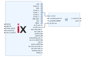
The AXI4-Stream interface provided in the sandbox template can be used to retrieve the ADC samples as AXI4-Stream interfaces.
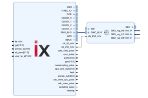
ADC interface
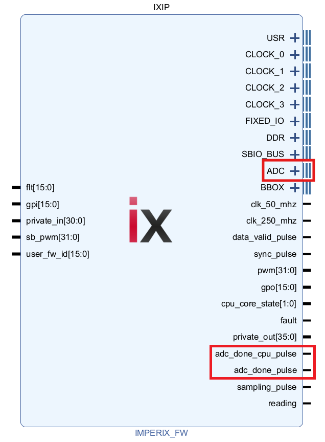
The ADC interface of the imperix firmware IP returns the raw ADC measurements in 16-bit signed integer format, as received by the ADC. The raw values therefore follow:
\[ \text{raw ADC value} = \text{controller input voltage} \;\times\; \frac{2^{15}}{\text{full scale}} \]
The full-scale voltage for each controller is indicated in the following table:
| B-Box 4 | B-Box RCP 3.0 | B-Box Micro, B-Board PRO |
| \(10\text{V}\) | \(10\text{V} \,/\; \text{programmable gain}\) | \(5\text{V}\) |
The adc_done_pulse signal indicates that the interface registers have been updated with new samples, effectively acting as a data valid strobe.
The adc_done_cpu_pulse is a decimated version of the adc_done_pulse. It indicates when the samples are also available to the user application running on the CPU. The relationship between these two pulses is therefore defined by the postscaler ratio.
The acquisition delay is defined as the time elapsed from the sampling pulse (sampling_pulse) to the corresponding data being available at the ADC interface (adc_done_pulse) when no filter is enabled (synchronous sampling). It is specified for each imperix controller in the table below.
| B-Box 4 | B-Box RCP 3.0 | B-Box Micro, B-Board PRO, TPI8032 | |
|---|---|---|---|
| Acquisition delay | 200 ns / 368 ns* | 2 μs | 500 ns |
* When channels A12-A23 are used.
ADC_FLOAT interface (B-Box 4 only)
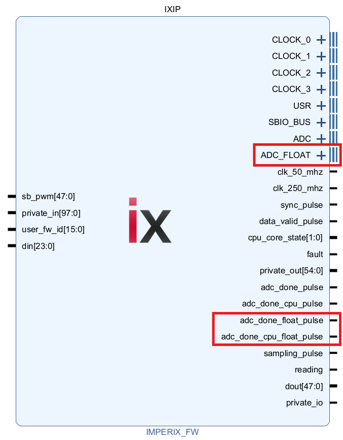
In the B-Box 4, the ADC_FLOAT interface provides access to the rescaled data as 32-bit registers in a floating-point format.
As already mentioned in the architecture description above, the rescaling offset and gain must be specified in the ADC block(s) in the user application.
Since rescaling induces an additional delay of 192 ns, the adc_done_float_pulse and adc_done_cpu_float_pulse valid pulses are provided. They are delayed versions of the adc_done_pulse and adc_done_cpu_pulse described in the ADC interface section above.
AXI4-Stream interface
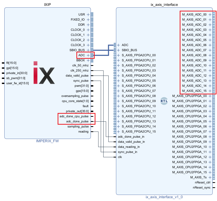
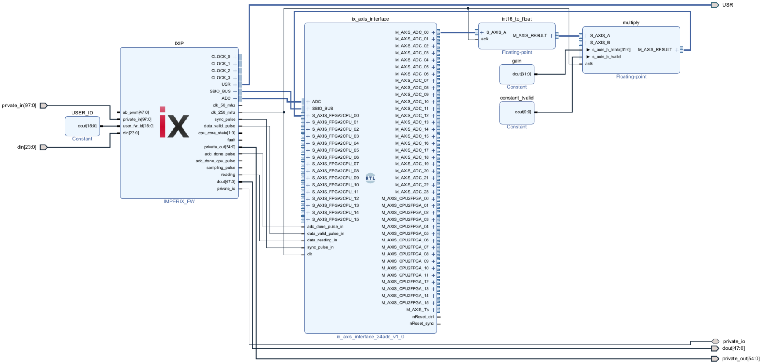
The AXI4-Stream interface module included in the sandbox template exposes the ADC measurements as AXI4-Stream interfaces. This enables the use of Xilinx AXI4-Stream IPs in the subsequent custom logic and facilitates the implementation of control algorithms, as illustrated in the example below.
The Master AXI4-Stream interfaces M_AXIS_ADC_00 to M_AXIS_ADC_15 correspond to the 16 analog inputs of the imperix device. They return the raw 16-bit signed integer in the same format as the ADC interface.
The CPU2FPGA and FPGA2CPU interfaces are documented in PN128 (Exchanging data between the CPU and the FPGA).
Example
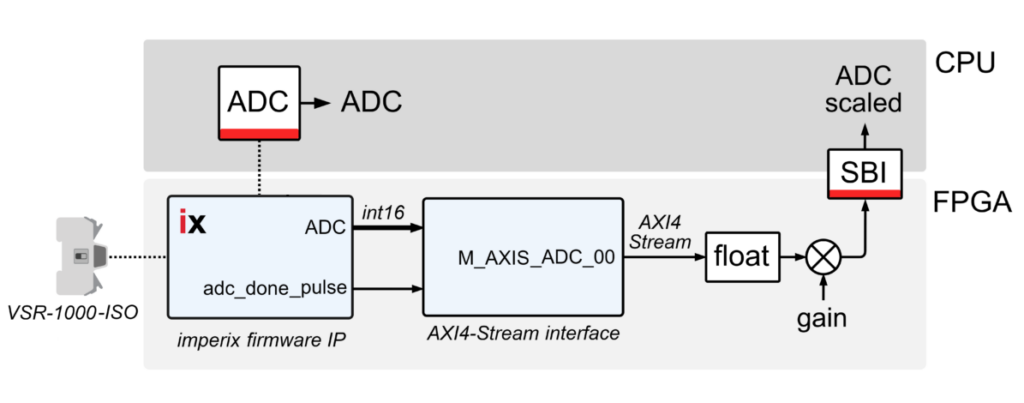
This example demonstrates how to access and process ADC measurements within the FPGA sandbox using exclusively IP provided by Vivado. Specifically, using a B-Box 4 controller and a VSR-1000-ISO voltage sensor, it illustrates how to:
- Retrieve ADC measurements from the imperix firmware IP via the provided AXI4-Stream interface.
- Convert the data from 16-bit signed integer to a 32-bit floating-point format using Xilinx floating-point IP configured for fixed-to-float operation.
- Multiply by the gain factor to convert raw data into their corresponding physical quantities using another floating-point IP configured for multiply operation.
- Send the result to the CPU for monitoring.
Gain computation
As explained in the ADC interface section, raw data follow:
\[ \text{raw ADC value} = \text{controller input voltage} \;\times\; \frac{2^{15}}{\text{full scale}} \]
where the full scale is 10V for the B-Box 4. With a sensor sensitivity of 5mV/V (see datasheet), the gain factor to be applied to the raw data to retrieve the physical voltage on the sensor’s terminals is:
\[ \text{gain} = \frac{1}{\text{sensor sensitivity}} \;\times\; \frac{\text{full scale}}{2^{15}} = \frac{1}{0.005} \;\times\; \frac{10}{2^{15}} = 61.04\cdot 10^{-3} \left[\frac{\text{V}}{\text{bit}}\right] \]
Step-by-step FPGA implementation
This section describes how to build the following FPGA design step by step.
Start from template
This example is based on the sandbox template provided in the imperix source files. Follow the procedure detailed in the Getting started page to get ready.
Add the int16-to-float converter
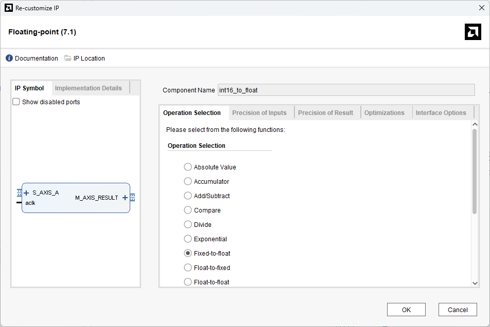
- Right-click somewhere in the block design, select Add IP and search for Floating-point. Press Enter.
- In the Block Properties panel, rename the block to int16_to_float.
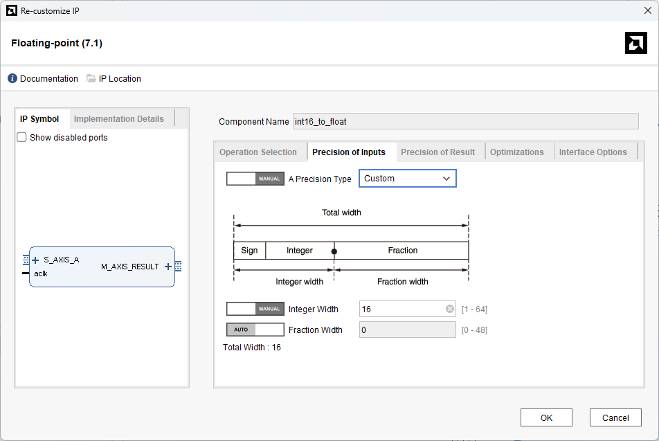
- Double-click on the IP to open the configuration panel. In the Operation Selection tab, select the Fixed-to-float operation. In the Precision of inputs tab, select Manual and Custom for the precision type. Then, select Manual for the integer width and set it to 16. Other parameters can be let in their default configuration.
Add the multiplier
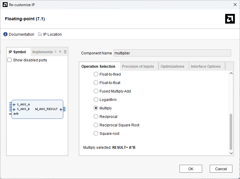
- Right-click somewhere in the block design, select Add IP and search for Floating-point. Press Enter.
- In the Block Properties panel, rename the block to multiplier.
- Double-click on the IP to open the configuration panel. In the Operation Selection tab, select Multiply for the operation. Other parameters can be let in their default configuration.
Add the two constants
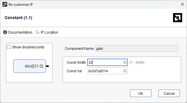
Because the constant block does not accept decimal values, the gain computed earlier (0.06104) must be converted to its hexadecimal representation (0x3D7A0514). This can be easily achieved using free conversion tools, such as this website.
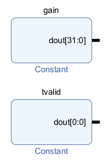
Moreover, the gain constant output is a static register, while the multiplier expects both operands to be provided as AXI4-Stream interfaces. A constant ‘1’ is therefore fed on tvalid, along with the gain on tdata, in the second input interface of the multiplier. This effectively transforms the static value into an (always-valid) AXI4-Stream.
- Right-click somewhere in the block design, select Add IP and search for Constant. Press Enter.
- Rename the block to gain. In the IP’s configuration panel, set the width to 32 and the value to 0x3D7A0514. This is the hexadecimal representation of the gain computed in the previous section, i.e., 0.06104.
- Add another Constant IP and rename it to tvalid. The default configuration with a width and value of 1 does not need to be changed.
Apply connections
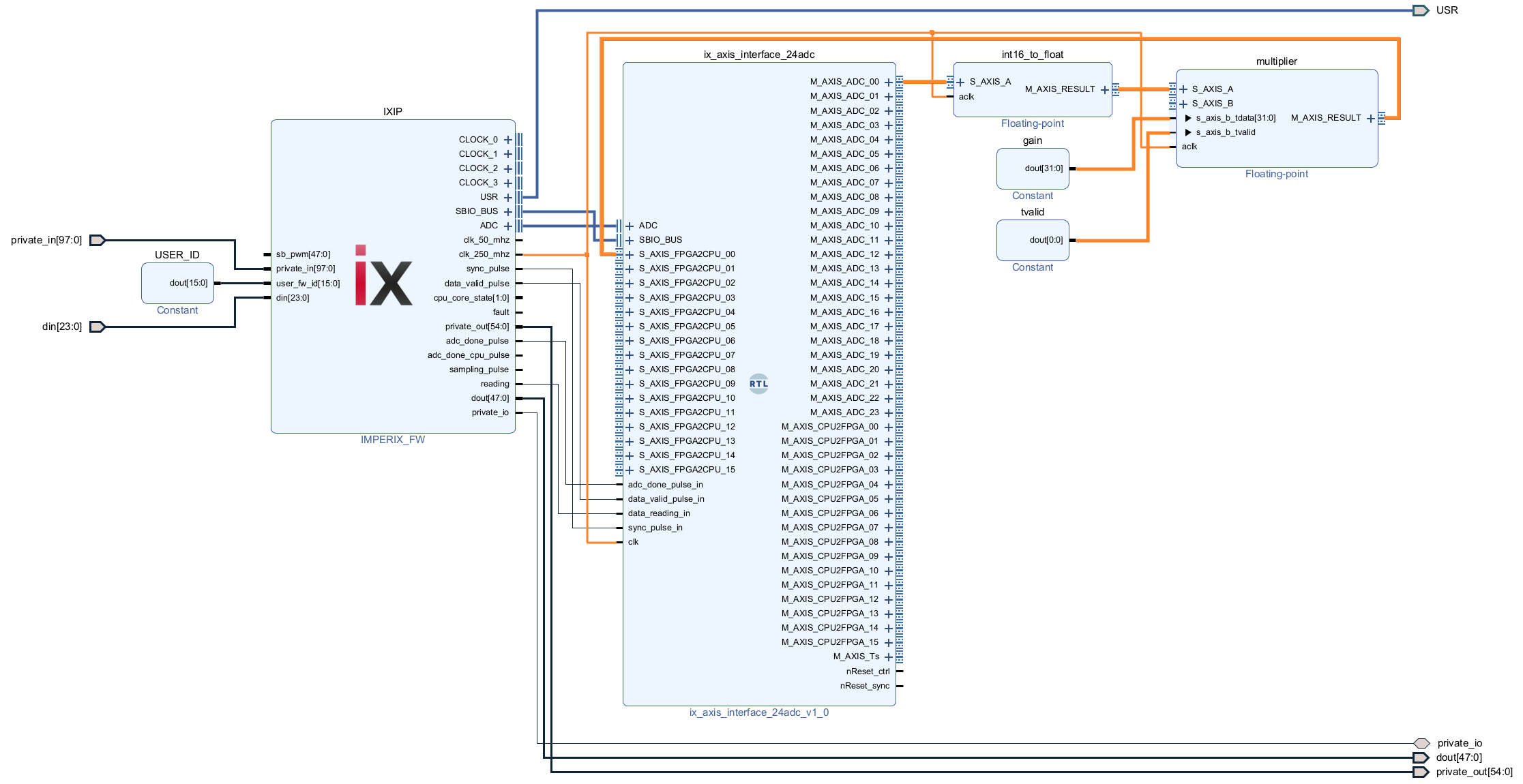
The design can be finalized by applying the following connections:
- ix_axis_interface/M_AXIS_ADC_00 interface to the int16_to_float/S_AXIS_A interface
- int16_to_float/M_AXIS_RESULT interface to multiplier/S_AXIS_A interface
- gain/dout signal to the s_axis_b_tdata signal of the multiplier/S_AXIS_B interface
- tvalid/dout signal to the s_axis_b_tvalid signal of the multiplier/S_AXIS_B interface
- multiplier/M_AXIS_RESULT interface to the ix_axis_interface/S_AXIS_FPGA2CPU_00 interface
- the two clocks signals (int16_to_float/aclk and multiplier/aclk) to the IXIP/clk_250_mhz signal
Save, build and load the design
- Save the design and click on Generate Bitstream in the sidebar on the left.
- Load the bitstream onto the controller via Cockpit.
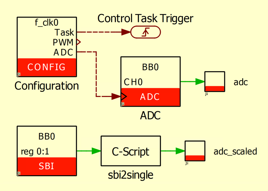
CPU model
The CPU model is provided below in Simulink and PLECS:
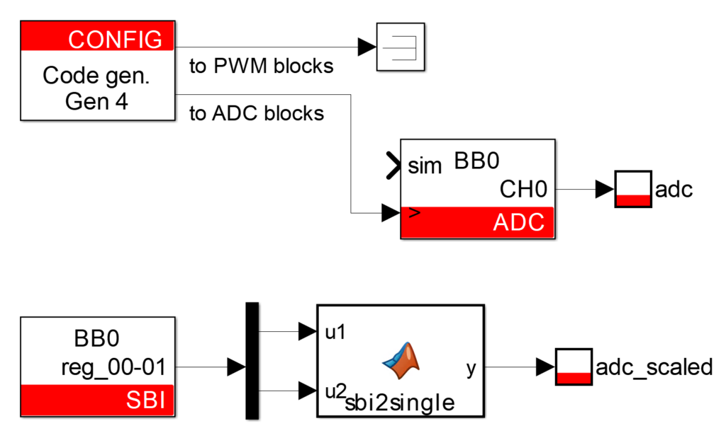
The user application contains:
- The CONFIG block where the sampling clock (SCLK) frequency, which is equal to the CLK0 frequency, is set to 20 kHz. The postscaler ratio kept to 1, meaning that the CPU and FPGA receive the ADC samples at the same rate.
- An ADC block, configured on channel 0 with a VSR-1000-ISO sensor. Synchronous averaging is activated.
- An SBI block to access the result computed in the FPGA from the CPU and monitor it in Cockpit. The sbi2single function converts the two 16-bit SBIO addresses into one 32-bit floating-point variable. More information about the CPU-FPGA communication is available in Exchanging data between the CPU and the FPGA.
Experimental validation
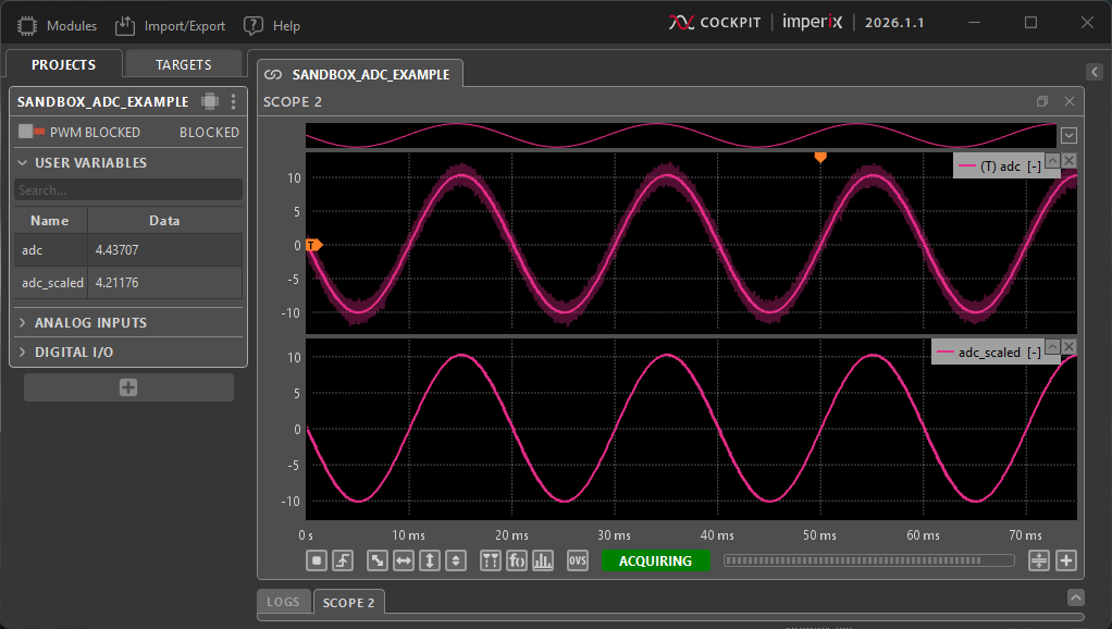
To validate this example, a sinusoidal voltage source has been connected to the voltage sensor terminals. The sensor output is connected to the ADC channel 0 (A0) of the B-Box.
Once the bitstream is loaded (the loading procedure is detailed here), the user application can be compiled (Ctrl+B in Simulink, Ctrl+Alt+B then Build in PLECS). Following compilation, Cockpit is automatically launched. The project can be linked to the controller and scopes can be added to the graphical interface to monitor the signals of interest. The Cockpit interface should appear as follows:
Going further
Using the Floating-point IP provided by Xilinx is convenient for simple operations, such as multiplying by a gain as demonstrated in the example above. For more complex algorithms, however, utilizing High-Level Synthesis (HLS) tools greatly facilitates the development process.