Table of Contents
This technical note provides an example of how a fast hysteresis current controller can be implemented, leveraging the possibility of editing the FPGA firmware for rapid control prototyping applications.
This example implements the direct current control of a three-phase passive load. It relies on manually-generated VHDL code. The automated generation of VHDL code is presented in TN121, which addresses the same application from Simulink and using Matlab HDL Coder.
Instructions on how to set up the FPGA development toolchain for imperix controllers are given in the dedicated note PN168. Quick-start recommendations regarding FPGA firmware customization can also be found in the getting started with FPGA control.
Software resources
The first file is the Simulink model used to generate the CPU code, and the second file contains a Vivado project that implements the FPGA logic described below.
Implementation of the hysteresis current control
This implementation stems from the following choices:
- The current references are generated inside the CPU at a 40 kHz interval.
- The measured 3-phase currents are sampled at 400 kHz.
- The hysteresis control is implemented inside the programmable logic area (FPGA) by comparing the “fast” measured currents (400 kHz) with the “slow” generated references (40 kHz).
- The hysteresis comparators are 2-level comparators.
- The PWM output states are directly derived from the comparator state (see logic below).
- A counter prevents the PWM output from switching excessively rapidly between states (state change limiter). This ensures that the switching frequency of each phase is kept below a defined threshold.
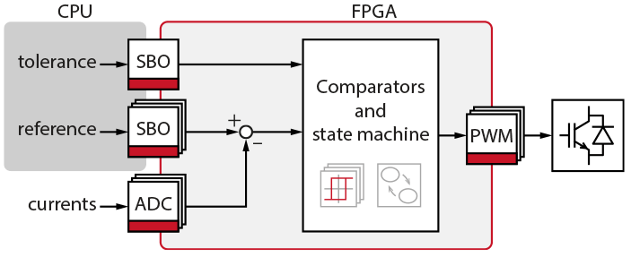
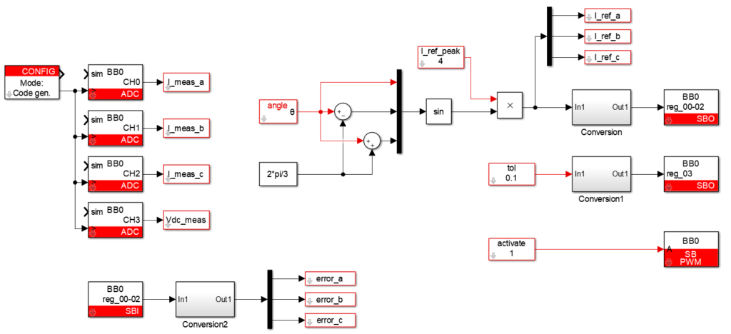
Both CPU and FPGA tasks are illustrated below. The current references and the tolerance values are computed in the CPU and transferred to the FPGA with SBO blocks.
FPGA logic of the hysteresis controller
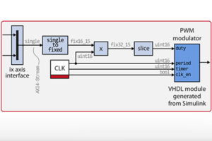
The following control logic is implemented in VHDL. Details on how to edit the firmware of the B-Box RCP are given in PN116.
The resulting logic is illustrated in the figure below. The current error is simply obtained by comparing the current reference with the actual measurement. Subsequently, as basic state machine controls the state transitions of the pwm_out signal, enforcing a minimum delay to limit the converter switching frequency.

This subsystem is instantiated three times, one for each phase. Connections are made as shown in the next figure:
meas_inare connected toADC_reg_00,ADC_reg_01andADC_reg_02ref_inare connected toSBO_reg_00,SBO_reg_01andSB0_reg_02tol_inare connected toSBO_reg_03delay_inare connected toSBO_reg_04err_outare connected to aSBI_reg_00,SBI_reg_01andSBI_02pwm_outare connected tosb_pwm[0],sb_pwm[2]andsb_pwm[4]

CPU implementation (using the imperix blockset for Simulink)
The following configuration is used:
- CLOCK_0 (main clock, controlling the sampling frequency): 400 kHz
- Interrupt postscaler: 5 (i.e. control interrupt executed at 40 kHz)
- SBO registers 00 to 02: current references (real-time registers)
- SBO register 03: hysteresis tolerance (real-time register)
- SBO register 04: state counter period (configuration register)
- SBI registers (read from FPGA) 00 to 02: current errors (for monitoring purpose only)
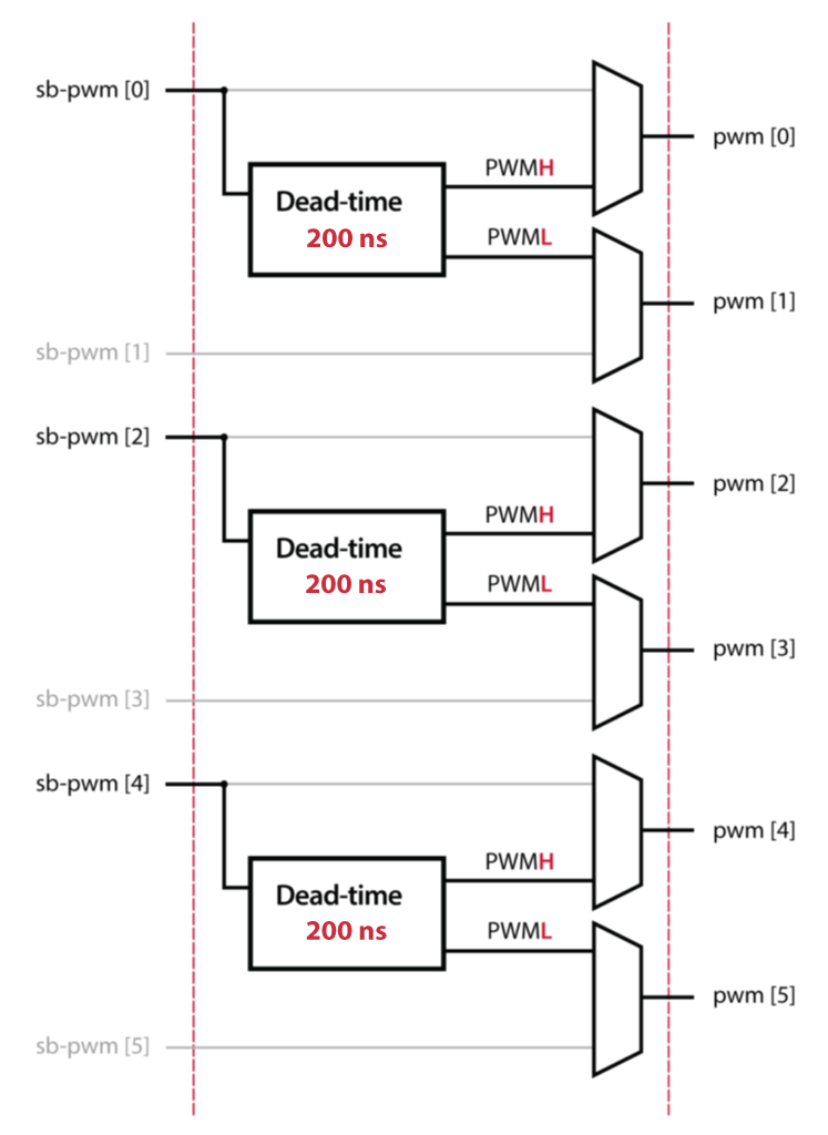
- SB_PWM: PWM channels 0 to 2 configured with dual outputs with a 1 us dead time
- State change limiter: maximum switching frequency: 40 kHz (i.e. H2L and L2H states have a counter period of 3125. Counter period is 4 ns)
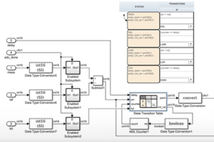
The CPU code is generated automatically from Simulink, using the following model:
The PWM output configuration is the following. Further information on sandbox PWM configuration is available on the custom FPGA PWM page.

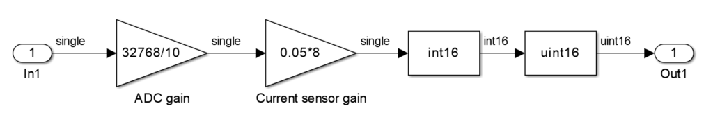
This model generates 3-phase current references with a user-defined amplitude and a frequency of 50Hz. These references are then converted into unsigned int16 format to match the format of the FPGA registers. The conversion from Amperes to bits or inversely is done with the following operations. It considers the sensitivity of the current sensors and an input voltage range of ±10V with 16 bits ADCs. The intermediate conversion to int16 ensures that the signed float number is coded or interpreted correctly in 2’s complement.

All probe variables are used for monitoring and debug purposes only.
Experimental results and validation of the hysteresis current control
The subsequent results consider the following parameters:
- VDC = 70 V
- Lload = 5 mH
- Rload = 8 Ohm
The resulting current waveforms are shown below, for a current reference of 4 A peak and a hysteresis tolerance of ±0.3 A and ±0.1 A :
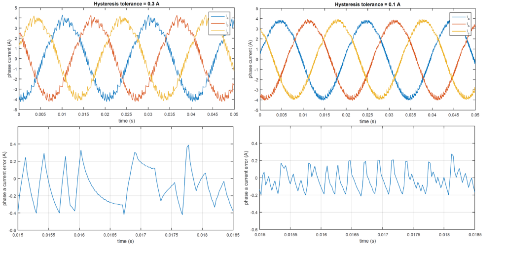
It can be clearly seen that reducing the hysteresis tolerance reduces the current ripples but increases the switching frequency. It also appears that the current error is not kept fully within the hysteresis band. This is unavoidable in digital implementations, for the following 2 reasons:
- A finite sampling frequency implies a maximum delay of Ts. In the present implementation, this corresponds to an additional current error of at most 1.5*VDC*Ts/Lload = 50 mA
- The ADCs have a non-zero conversion delay. In the present implementation, the ADC have a 2 µs delay, which leads to an additional current error of at most 1.5*VDC*Tdelay/Lload = 42 mA
All in all, this explains a current error of approx. 100 mA beyond the hysteresis bounds.