Table of Contents
High-level synthesis (HLS) tools greatly facilitate the implementation of complex power electronics controller algorithms in FPGA. Indeed HLS tools allow the user to work at a higher level of abstraction. For instance, the user can use Xilinx Vitis HLS to develop FPGA modules using C/C++ or the Model Composer plug-in for Simulink to use graphical programming instead.
This page shows how IPs generated using high-level synthesis tools can be integrated into the FPGA of an imperix power controller. To this end, the example of a PI-based current controller for a buck converter is used to illustrate all the required steps.
Integrating HLS designs in the FPGA
Description of the design
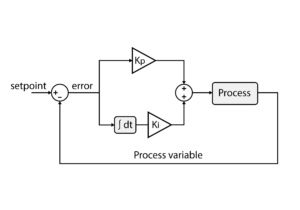
The image below shows the example that will be implemented on this page. It is a PI-based current controller for a buck converter, based on the algorithm presented on the PI controller implementation for current control technical note. This example uses the following resources
- the FPGA control starter template from the getting started with FPGA guide
- the PWM modulator IP from the FPGA PWM modulator example
- the high-level synthesis PI-based current control IP from either
- the C++ implementation presented in the Xilinx Vitis HLS guide
- or the Simulink implemention presented in the Model Composer guide
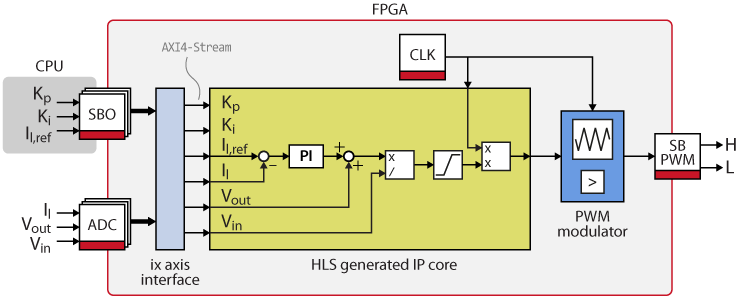
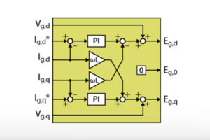
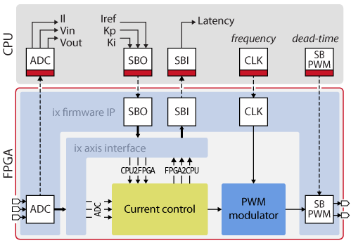
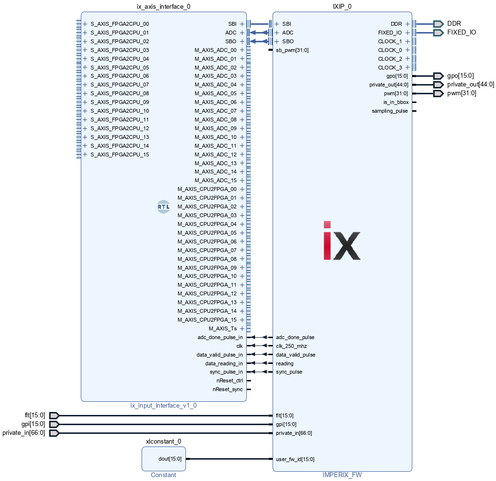
The axis interface provides the inputs of the current control algorithm in form of AXI4-Stream ports. The following ports are used:
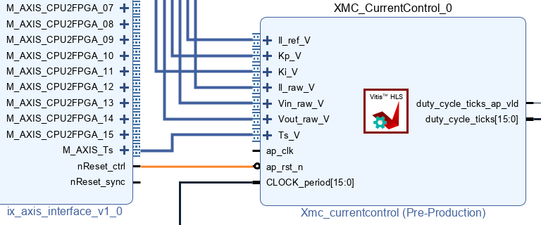
CPU2FPGA_00for the current referenceIl_ref(32-bit single-precision)CPU2FPGA_01for the parameterKp(32-bit single-precision)CPU2FPGA_02for the parameterKi(32-bit single-precision)ADC_00for the measured currentIl(16-bit signed integer)ADC_01for the measured output voltage of the converterVout(16-bit signed integer)ADC_02for the measured input voltage of the converterVint(16-bit signed integer)Tsfor the sampling period in nanoseconds (32-bit unsigned integer)
Aside from AXI4-Stream data, the current control IP also uses the ports:
CLOCK_periodfor the PWM period in ticks (16-bit unsigned)nReset_ctrlto reset the PI when the controller is not in OPERATING state
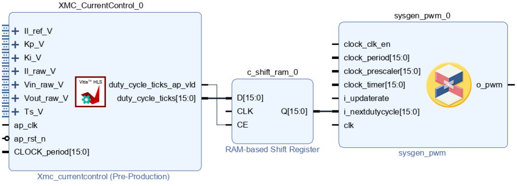
Using these signals, the HLS IP computes a 16-bit unsigned duty_cycle_ticks that is forwarded to the PWM IP. And finally, the PWM IP uses the sb_pwm driver to output the PWM signals to optical fibers of the B-Box RCP controller. The PWM IP and the SB-PWM driver are further documented on the FPGA PWM modulator page.
CPU-side implementation using Simulink
The CPU-side model is quite simple, as the control algorithm runs entirely in the FPGA. The CPU code provides the current reference and Kp/Ki parameters, operates the PI reset signal, and configures the PWM outputs.
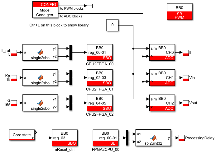
The single2sbo MATLAB Function blocks are used to map the current reference Il_ref and the Kp, Ki parameter to the CPU2FPGA ports.
This nReset_ctrl signal is used to keep the PI integrator at reset when the controller is not in OPERATING state. As documented in Getting started with FPGA, this reset signal is controlled using SBO_63. To obtain the desired behavior, we’ll simply connect the reset output of a Core state block to SBO_63.
And finally, the SB-PWM block is used to activate the output PWM channel 0 (CH0) (lane #0 and lane #1). The output is configured as Dual (PWM_H + PWM_L) with a deadtime of 1 µs. This configuration expects a PWM signal coming to sb_pwm[0] input of the imperix firmware IP and will automatically generate the complementary signals with the configured deadtime.
The ADC blocks are only used to retrieve the analog input signals at the CPU level for real-time monitoring. They do not affect the closed-loop control behavior.
FPGA-side implementation using Vivado
The TN142_vivado_design.pdf file below shows the full Vivado FPGA design. Here are the step-by-step instructions to reproduce it.
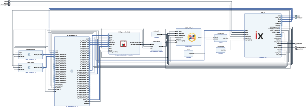
- Create an FPGA control implementation starter template by following the Getting started with FPGA control implementation.
- Add the PWM IP (from the custom PWM in FPGA page) and current control IP (from the Xilinx Vitis HLS guide or the Model Composer guide) into your Vivado project. In the screenshots of this example, we’ll use the IPs generated using System Generator and Vitis HLS, respectively.
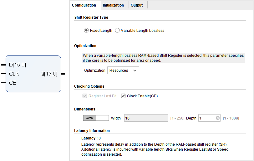
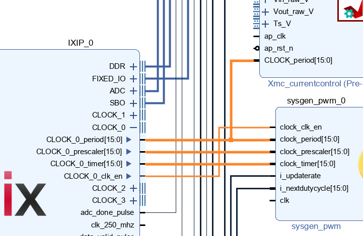
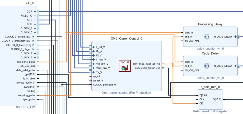
To read theduty_cycle_ticksonly whenduty_cycle_ticks_ap_vldis ‘1’, the RAM-based Shift Register IP is used. With the configuration shown in the screenshot below, this block adds one register stage that acts as a buffer. It keeps the last computed duty cycle until a new value has been computed. When a new value is available, it replaces the old one.
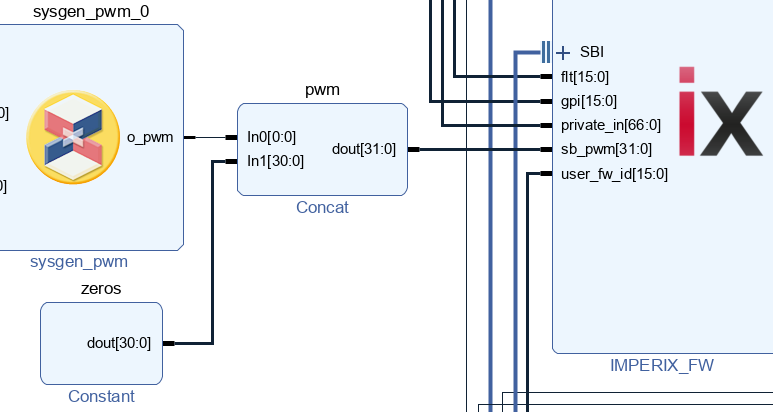
- Add a Constant IP to set all the 31 unused sb_pwm outputs to ‘0’. Set its Const Width to 31 and its Const Val to 0.
- Add a Concat IP. It will serve to concat the pwm output of the PWM IP with the zeros of the Constant IP.
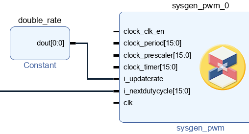
- Add a Constant IP to set to set the update rate. ‘0’ = single rate, ‘1’ = double rate.
- Connect the clock signals as below:
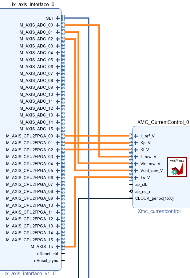
- Connect the AXI4-Streams
M_AXIS_CPU2FPGA_00toIl_ref_VM_AXIS_CPU2FPGA_01toKp_VM_AXIS_CPU2FPGA_02toKi_VM_AXIS_ADC_00toIl_raw_vM_AXIS_ADC_01to voltageVout_raw_VM_AXIS_ADC_02toVint_raw_VM_AXIS_TstoTs_V
- The provided Delay Counter VHDL module (delay_counter.vhd) measures the elapsed time between two signals and outputs a time in nanoseconds, encoded as a uint32.
In this design, the delay counter modules are used purely for debugging purposes. As shown in the image below, one is used to measure the FPGA processing delay, which is the delay between theadc_done_pulseand theduty_cycle_ticks_ap_vld. Another module is used to measure the FPGA cycle delay by measuring the delay between thesampling_pulseand theduty_cycle_ticks_ap_vld. More information on what these delays represent are available on the discrete control delay product node.
- Connect the
nReset_ctrlsignal toap_rst_n.
- And finally connect the clk signals to
clk_250_mhz. - Click Generate bitstream. It will launch the synthesis, implementation, and bitstream generation
- Once the bitstream generation is completed, click on File → Export → Export Bitstream File… to save the bitstream somewhere on your computer.