Table of Contents
Beyond the built-in modulators accessible from the user application, the imperix sandbox enables PWM generation directly within the FPGA, allowing for the implementation of custom modulation strategies.
Within the sandbox, this process is simplified by the availability of the built-in clocks (CLK0, CLK1, CLK2, CLK3), which are configured via the user application and shared across the entire system. Utilizing these shared clocks ensures perfect synchronization between the FPGA modulator, CPU sampling, and other system components.
For convenience, the sandbox source files include a ready-to-use carrier-based modulator written in VHDL. The example at the end of this page details the integration of this modulator into a functional FPGA design.
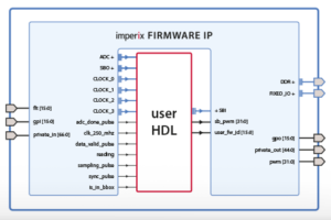
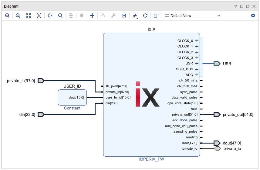
Customizing the FPGA firmware involves instantiating the imperix firmware IP within Xilinx Vivado to edit the surrounding programmable logic, known as the sandbox. For step-by-step instructions on creating the required FPGA sandbox template, refer to the getting started guide.
The PWM chain
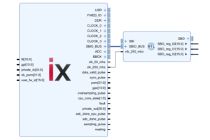
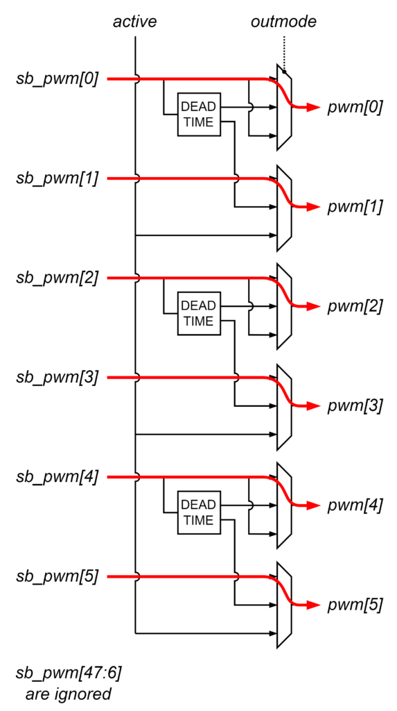
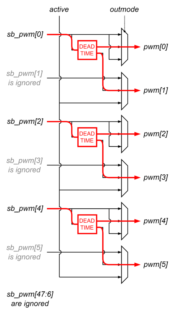
In the FPGA, the PWM signals are be driven via the sb_pwm port of the imperix firmware IP.
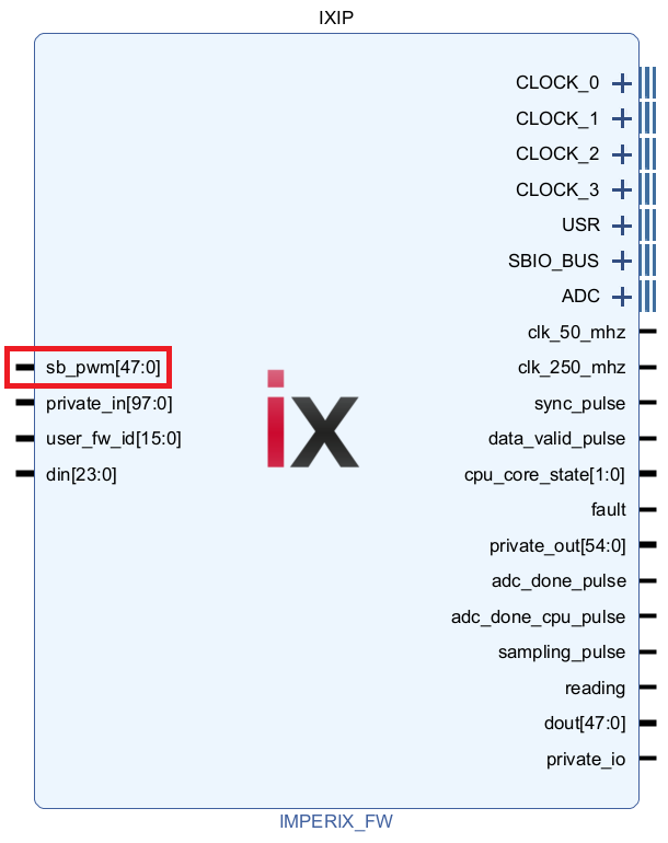
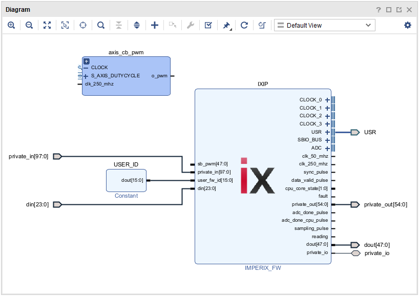
As shown below, the signals fed through the sb_pwm port of the imperix firmware IP (IXIP) are considered as an additional PWM source, equivalently to the output of all built-in modulators. This means that the dead-time generation, activation and protection mechanisms are also available when driving the PWM from the sandbox.
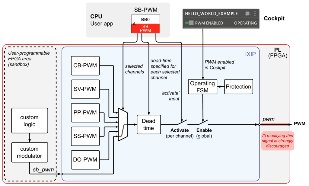
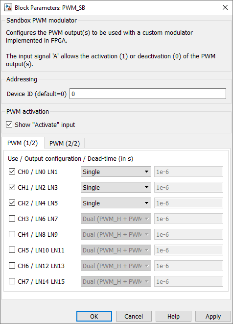
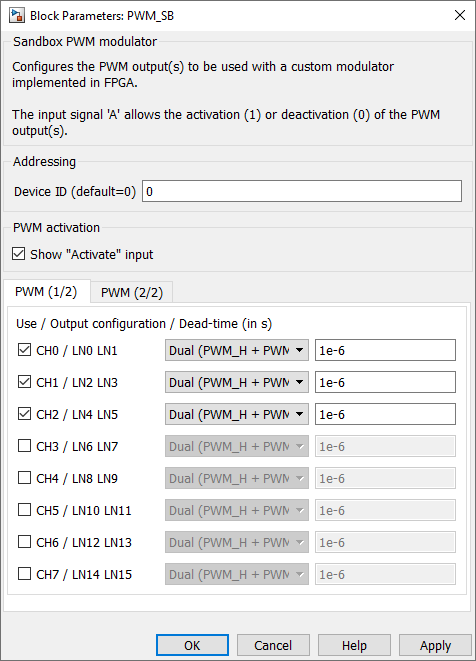
pwm port, as this would bypass the protection mechanism. Instead, PWM signals from the sandbox should be routed through the sb_pwm input port.To drive PWM outputs from the sandbox, the corresponding channels must be selected using an SB-PWM block in the user application. For each selected channel, this block also indicates:
- The output mode (usually single or dual).
- The dead-time to be applied for each channel set as dual.
Single mode
Dual mode
A third output mode, called PWM + ACTIVE, is also available for very specific use cases. In this mode, the first lane of each channel behaves as the single mode, while the second lane indicates if the channel is active (PWM activated and enabled) or not.
The following table summarizes the mapping of the channels (or lanes) for the three available output modes.
| PWM output | source of the PWM output | ||||
| channel | pin | single | dual (PWM_H+PWM_L) | dual (PWM+ACTIVE) | |
| CH0 | pwm(0) | sb_pwm(0) | dead-time(sb_pwm(0)) | H signal | sb_pwm(0) |
| pmw(1) | sb_pwm(1) | L signal | channel active signal | ||
| CH1 | pmw(2) | sb_pwm(2) | dead-time(sb_pwm(2)) | H signal | sb_pwm(2) |
| pmw(3) | sb_pwm(3) | L signal | channel active signal | ||
| CH2 | pmw(4) | sb_pwm(4) | dead-time(sb_pwm(4)) | H signal | sb_pwm(4) |
| pmw(5) | sb_pwm(5) | L signal | channel active signal | ||
| … | … | … | … | ||
| CH23 | pwm(46) | sb_pwm(46) | dead-time(sb_pwm(46)) | H signal | sb_pwm(46) |
| pmw(47) | sb_pwm(47) | L signal | channel active signal | ||
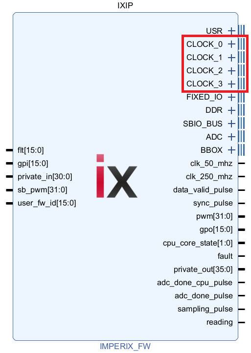
The CLOCK interface
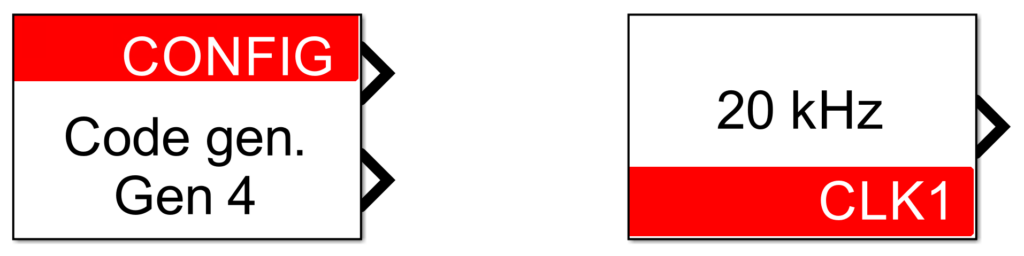
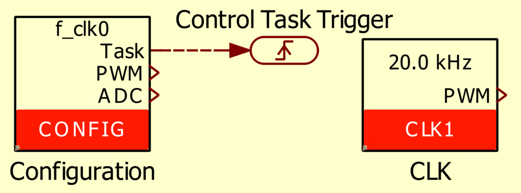
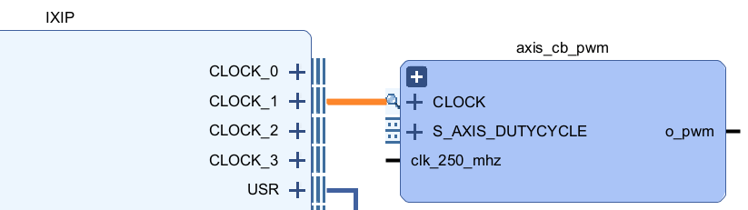
The modulators implemented in the sandbox can rely on the same built-in clocks than the other built-in modulators: CLK_0, 1, 2, 3. These clocks are configured via the CONFIG (CLK_0) or CLK (CLK_1, 2, 3) blocks in the user application.
In the FPGA, the clocks can be accessed through the CLOCK_0, 1, 2, 3 interfaces on the imperix firmware IP (see right picture below). These interfaces can be directly connected to custom modulators in the sandbox, as shown in the example below where CLK_1 is used to drive the modulator in the FPGA.
in Simulink.
in PLECS.
Using the built-in clocks spares users from having to implement their own clock generation logic, guarantees the switching synchronization with the other internal modulators, and allows for easy frequency adjustments from the user application without the need to regenerate a new bitstream.
CLOCK_period, CLOCK_timer, CLOCK_prescaler and CLOCK_clk_en. More information about the interface signals is available in the IXIP product guide.Provided carrier-based modulator
Since it is not possible to directly drive the built-in CB-PWM modulators from within the sandbox, it is required to instantiate a PWM modulator within the FPGA. For convenience, a carrier-based modulator written in VHDL is provided in the imperix source files. This modulator, shown below, is directly inspired from the built-in CB-PWM modulator.
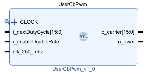
The modulator uses a pulse-width modulation based on a triangular carrier. The carrier is generated from the clock interface, which must be connected to one of the four CLOCK interfaces of the firmware IP in the FPGA and configured from the user code (see previous section).
The duty cycle can be updated using a single rate or double rate. When using the single-rate update, the duty cycle value is applied when the triangular carrier reaches its minimum. With the double-rate update, the duty cycle is updated twice per period: when the carrier reaches its maximum and when it reaches its minimum.
Pinout
| Port name | Direction | Width | Description |
CLOCK_period | IN | 16 | Period of the clock used to generate the PWM carrier, expressed as an number of ticks (1 tick = 4*CLOCK_prescaler ns).E.g. a clock set to 20 kHz results in CLOCK_period = 12500 ticks. |
CLOCK_timer | IN | 16 | Counter of the clock used to generate the PWM carrier, counting from 0 to CLOCK_period-1 at a rate of 250MHz/CLOCK_prescaler.The triangle carrier: – is reset to 0 when CLOCK_timer=0– goes up while CLOCK_timer < CLOCK_period/2-1.– goes down while CLOCK_timer >= CLOCK_period/2-1. |
CLOCK_prescaler | IN | 16 | Indicates the used prescaler division value for the CLOCK. |
CLOCK_clk_en | IN | 1 | Clock enable signal indicating when CLOCK_timer was incremented.When CLOCK_prescaler > 1, CLOCK_clk_en is asserted once every N cycles (where N = CLOCK_prescaler) |
i_nextDutyCycle | IN | 16 | Desired duty-cycle for the PWM signal, expressed as an number of CLOCK_period ticks. It ranges from 0 to i_nextDutyCycle-1. |
i_enableDoubleRate | IN | 1 | Selection of the single update rate (0) or double update rate (1). |
clk_250_mhz | IN | 1 | Main clock running at 250 MHz. |
o_pwm | OUT | 1 | PWM signal generated by the modulator. |
o_carrier | OUT | 16 | Access to the internal carrier used to generate the PWM signal, for monitoring or debug purposes. |
AXI4-Stream carrier-based modulator
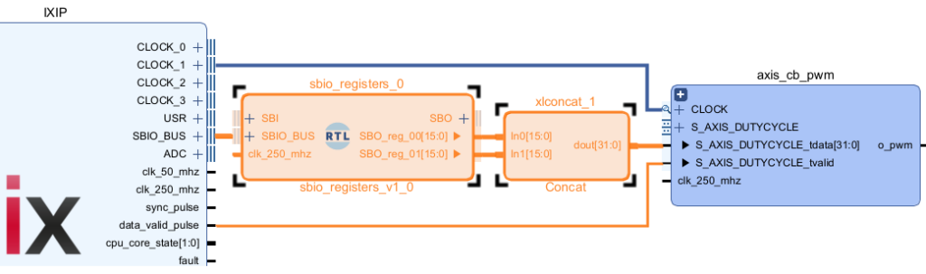
To facilitate the use of the carrier-based modulator described above, an extended version is provided called axis_cb_pwm. This variant accepts a 32-bit floating-point duty cycle, ranging from 0.0 to 1.0, via an AXI4-Stream interface.
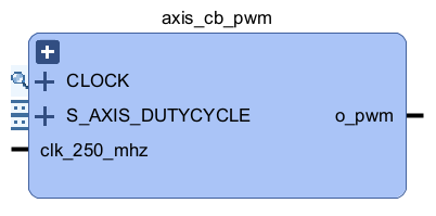
As shown below, the axis_cb_pwm was implemented using standard Vivado IPs and is distributed as a hierarchical Block Design. This approach is intended for educational purposes, allowing users to easily navigate and modify the underlying structure.
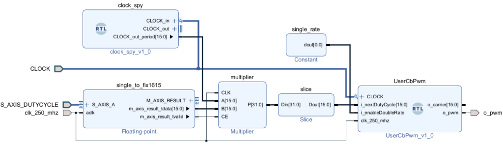
The blocks are the following:
- single_to_fix16_15: The 32-bit single-precision floating-point value is transformed into a 16-bit fixed-point value with an integer width of 1-bit and a fraction width of 15-bit (fix16_15). This repartition has been chosen because the duty cycle is expected to range between 0.0 and 1.0 so only 1-bit is required on the integer part.
- clock_spy: serves to extract the
CLOCK_periodsignal from the CLOCK interface. - multiplier: To obtain a value in ticks, the result of the previous step is multiplied by
CLOCK_period. The result of the multiplication of a fix16_15 with a uint16 is a fix32_15 (32-bit, 17-bit integer part, and 15-bit fractional part). The clock enable (CE) input is enabled and connected to the tvalid output of the single_to_fix16_15 IP output. This way, the multiplication is performed synchronously with the data coming from the AXI4-Stream. - slice: Only the 16 first bits of this result are used as the duty cycle input of the FPGA PWM modulator IP.
- UserCbPwm: The carrier-based modulator provided with the FPGA sandbox template sources.
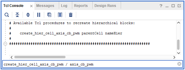
A Tcl script to re-create an axis_cb_pwm module is provided below.
The procedure to use it is as follow:
- Download axis_cb_pwm.zip and unzip it.
- Copy
axis_cb_pwm/hdl/clock_spy.vhdinto<path-to-project>/hdl/ - Copy
axis_cb_pwm/scripts/axis_cb_pwm.tcl<path-to-project>/scripts/ - Add
clock_spy.vhdandUserCbPwm.vhdto the Vivado project using Add Sources. - In Vivado Tcl Console, type
source <path-to-project>/scripts/axis_cb_pwm.tclto load the script. - In Vivado Tcl Console, type
create_hier_cell_axis_cb_pwm / <desired_name>to create an axis_cb_pwm.
Example
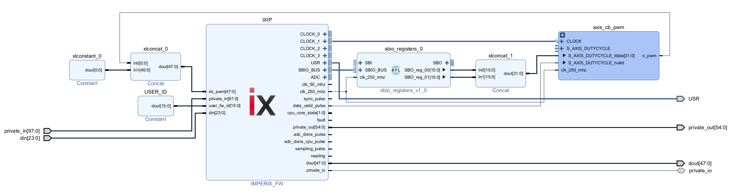
This example illustrates how to insert the provided PWM modulator within a functional FPGA design, which receives the duty-cycle from the CPU user application. It was made for the B-Box 4, using the imperix firmware IP 4.0 Rev 0.
1. Create an empty project
- Create the Vivado sandbox template following the “Creating the Vivado sandbox template” procedure detailed in the Getting started.
- Remove the AXI4-Stream interface by clicking on ix_axis_interface and pressing Delete.
2. Instantiate an AXI4-Stream carrier-based PWM module
- Download and unzip axis_cb_pwm.zip provided above.
- Copy
axis_cb_pwm/hdl/clock_spy.vhdintoexample_pwm/hdl/ - Copy
scripts/scripts/axis_cb_pwm.vhdintoexample_pwm/scripts/ - Add
clock_spy.vhdandUserCbPwm.vhdto the Vivado project using Add Sources.
- In Vivado Tcl Console, type
source <path-to-project>/scripts/axis_cb_pwm.tclto load the script then type typecreate_hier_cell_axis_cb_pwm / <desired_name>to create an axis_cb_pwm
3. Connect the PWM module frequency to CLOCK_1 so it can be changed using the CLK block
- Connect the PWM module to CLOCK_1.
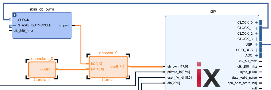
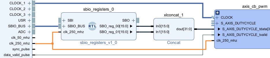
4. Output the PWM signal to Channel D0 (lanes 0 and 1)
- Connect the
o_pwmoutput tosb_pwm[0]. Setsb_pwm[1]tosb_pwm[47]to 0.
5. Connect S_AXIS_DUTYCYLCE interface to the CPU
As explained in the example description, the AXI4-Stream is not used in this example because of the additional delay that it introduces on the CPU-to-FPGA signals. Instead, two SBO registers are concatenated to obtain a 32-bit value that can be written from the CPU.
- Add
sbio_register.vhdto the Vivado project using Add Sources. - Instantiatean sbio_register module.
- Concatenate
SBO_reg_00andSBO_reg_01and connect the result toS_AXIS_DUTYCYCLE_tdata. - Connect
data_valid_pulsetoS_AXIS_DUTYCYCLE_tvalid.
6. Finally, connect the clk signals.
Experimental validation
The CPU model is provided below in Simulink and PLECS.
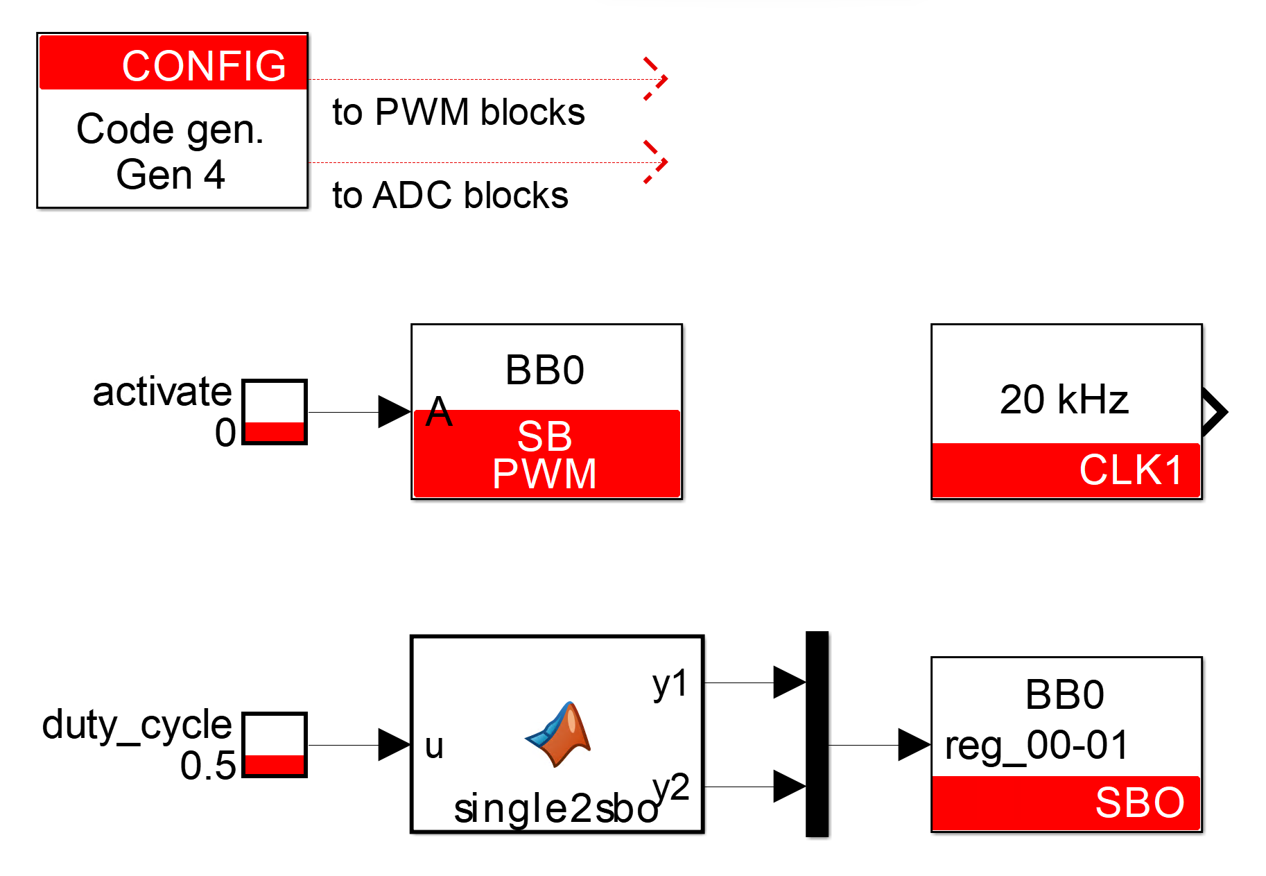
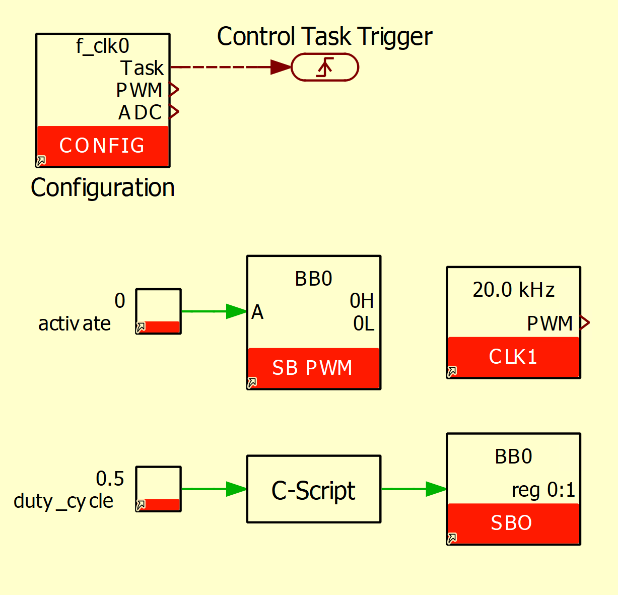
Along with the CONFIG block, the user application contains:
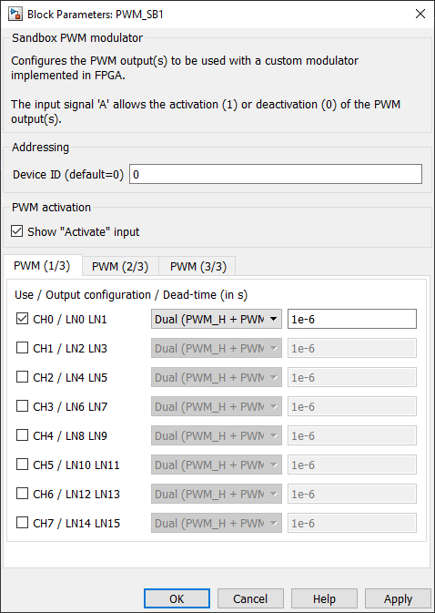
- An SB-PWM block with the configuration shown on the picture (right). It indicates that the source of channel 0 (CH0, LN0 LN1) must be taken from the sandbox and configures the dead-time to 1 us. The activate block input is set as visible and driven by a tunable parameter.
- A CLK block, where the clock CLK1 is set to 20 kHz. This clock drives the custom modulator in the FPGA.
- A MATLAB function (Simulink) or C-Script (PLECS) with an SBO block to convert the duty-cycle into two uint16 values and send the values to the FPGA. More information about the CPU-FPGA communication is available here.
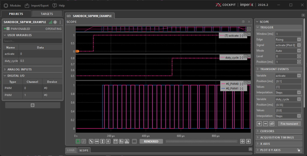
The figure below shows the result, obtained by controlling the activate and duty-cycle values via the built-in Cockpit transient generator. The duty-cycle is 0.5 by default, then changed to 0.8 after 0.55 ms. As expected, PWM outputs are clamped to 0 until the activate signal is asserted after 0.1 ms.
For other imperix controllers, electrical PWM outputs can be monitored with an oscilloscope.
Going further
Debugging an FPGA module
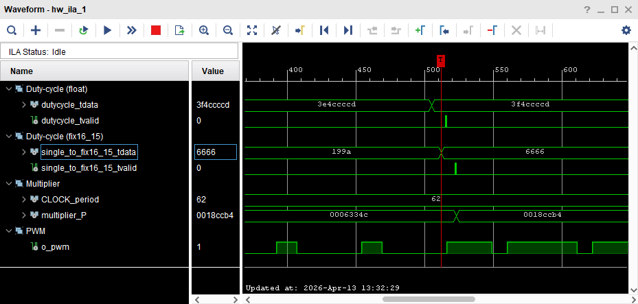
When designing a PWM modulator or other peripherals within the FPGA, it is highly useful to capture and observe internal FPGA signals similar to a simulation environment. PN129 explains how to capture these signals using a Xilinx Integrated Logic Analyzer (ILA), like shown in the screenshot below.
Using automated code generation to avoid writing VHDL
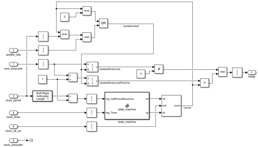
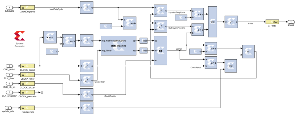
The provided carrier-based modulator is written in VHDL. It is possible however to achieve the same functionality without writing a single line of HDL code. As illustrated on the screenshots below, automated code generation tools such as AMD Vitis Model Composer and MATLAB HDL Coder can be used to create the same modulator using MATLAB Simulink.
The following pages explain how to re-create the same modulator using these tools:
- Carrier-based PWM using MATLAB HDL Coder
- Carrier-based PWM using AMD Vitis Model Composer HDL (formerly System Generator, or SysGen)