

Table of Contents
This technical note presents an implementation example of the TPI 8032 programmable inverter, operated as a Grid-Forming Inverter (GFMI). It provides a concise overview of the operating principle and offers a comprehensive guide to tuning the cascaded AC voltage control system used in this setup.
An overview of the hardware architecture and instructions for programming the device are provided in PN190.
Grid-Forming Inverter overview
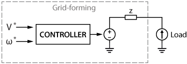
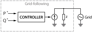
Grid-forming inverters (GFMI) and grid-following inverters (GFLI) are two basic categories of grid-connected inverters. Essentially, a grid-forming inverter works as an ideal voltage source that sets the amplitude \(V^{\star}\) and frequency \(\omega^{\star}\) of the grid. In contrast, a grid-following inverter works as a current source that synchronizes its output with the grid voltage and frequency and injects or absorbs active (\(P^{\star}\)) or reactive (\(Q^{\star}\)) power by controlling its output current [1].
Grid-forming inverters (GFMIs) are crucial in microgrid systems, particularly in islanded or isolated conditions. The concept of GFMIs originated from the need, in islanded mode, for at least one inverter designed to autonomously establish and maintain grid-like conditions, even without a centralized grid connection supplied by traditional synchronous generators. Unlike grid-following inverters, which synchronize with an existing grid, GFMIs act as the primary power source and create a self-sustainable grid environment. The voltage produced by a grid-forming inverter serves as a reference for the grid-following inverters connected to it [2].
Nonetheless, the voltage quality of a microgrid is not exclusively dependent on grid-forming inverters. Loads connected to the microgrid distribution lines can positively or negatively affect the voltage profile along the line. To this end, several grid-forming inverters, together with a droop control technique, can be employed to enhance voltage quality and improve the system’s reliability.
Control of grid-forming inverters
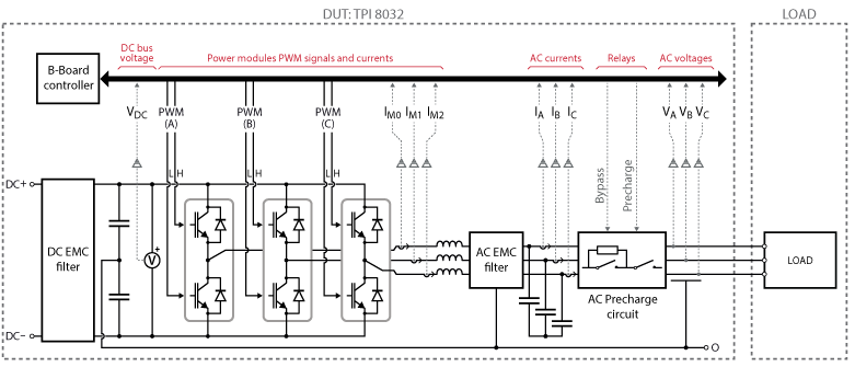
In this note, the control of the grid-forming inverter is introduced using the TPI 8032 as a programmable inverter. The schematic of the whole system is shown below together with the main plant parameters.
| Parameter | Value | Description |
|---|---|---|
| Lg | 1.0 mH | Main filter inductance |
| Rg | 54 mΩ | Series equivalent resistance of Lg |
| Cf | 12.9 µF | Filter capacitance |
Proper control of a GFMI should guarantee stable frequency, voltage, and power delivery to a generic load connected at the point of common coupling. This is achieved through the so-called VF control [3]. The control can be implemented through single-loop or dual-loop control. The main difference between the two is that the dual-loop control also provides current-limiting capability. The presented GFMI control consists of a dual-loop control implemented with PI controllers working in the dq reference frame. The control diagram can be represented as follows [3]:
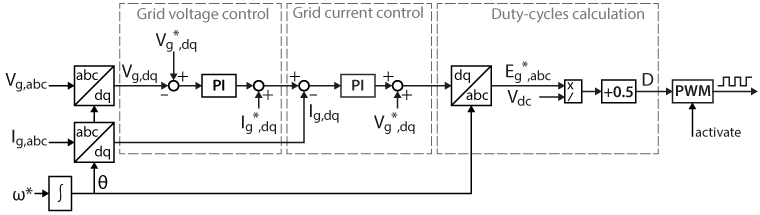
The system input is the amplitude \(V^{\star}\) and the frequency \(\omega^{\star}\) of the voltage to be formed by the power converter at the AC output terminals. The frequency reference is implemented directly within the angle generator block in the Simulink blockset, which is essentially a counter wrapped between 0 and 2π.
The external loop controls the AC grid voltage to match its reference value. The error between the reference and the measured voltage is the input to the PI voltage controller, whose output establishes the current reference to be injected by the converter. The internal control loop regulates the converter current by tracking the reference current from the outer voltage loop.
Plant model of the voltage and current controllers
The following equations present the transfer functions of the control loops. These transfer functions are based on the system’s plant model. They are necessary for tuning the inner and outer loops of the cascade voltage control. This process will be discussed in detail in the following Section.
The inner loop transfer function is:
$$ \frac{K}{1+sT_{d1}}\cdot\frac{1}{R_{b+}sL_{b}}$$
The outer loop transfer function is:
$$ \frac{K}{1+sT_{d,eq}}\cdot\frac{1}{sC_{f}}$$
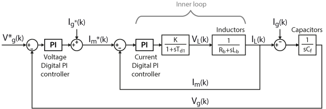
Once the different control loops have been properly identified, each state variable can be controlled separately. In this example, both control loops are proposed to be implemented using PI controllers in the rotating reference frame (dq). The design of the current control loop is detailed in TN167, whereas voltage control is further detailed in the following section.
Grid voltage control
The adopted voltage control loop is represented in the following schematic. Since the d- and q-axes are naturally coupled, a decoupling term is added to the PI controllers’ output. For a step change in d-voltage, a variation in the q-voltage is still expected. However, the decoupling term reduces the q-axis voltage variation, thereby providing more independent control over each axis.
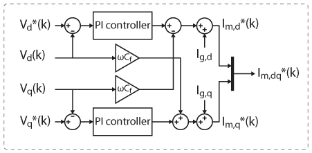
For the design of the voltage control loop, different methods are used in the literature [4]. In this article, the voltage control loop design is based on the Symmetrical Optimum (SO) method, as it provides well-established tuning-parameter design rules with an emphasis on stability. Indeed, as the objective of the voltage control loop here is rather perturbation rejection than tracking performance (setpoints are likely constant in dq frame), it is reasonable to optimize it for stability rather than bandwidth. The controller parameters are defined as follows:
$$\begin{array}{l}
T_{2} = C_{f} \\
T_{i2} = a^2 T_{d,eq}\end{array}
\qquad\text{and}\qquad
\begin{array}{l}
K_{p,V} = T_{2} /(a*T_{deq}) \\
K_{i,V} = K_{p,V} / T_{i2}
\end{array}$$
With \(T_{d,eq}\) the equivalent delay of the closed-loop current controller transfer function, defined as:
$$T_{d,eq} = 10 T_{d1}$$
In a voltage-current cascade control system, the voltage controller should be slower than the current controller. Therefore, the inner-loop delay is accounted for in the tuning of the outer loop. \(T_{d1}\) is multiplied by 10 to ensure that the voltage controller responds appropriately to changes in current, preventing overshoots or instability in the system.
The parameter \(T_{d1}\) represents the sum of all the small delays in the system. In this example, the cycle delay is shorter than half a control period (\(T_{cy}<0.5T_{s}\)), and a triangular carrier is used for PWM. Therefore, the following delays defined in PN142 are considered here:
- Sensor delay: neglected, several tens of kHz of bandwidth
- Control delay: \(T_{d,ctrl}=0.5T_{s}\)
- Modulator delay: \(T_{d,PWM}=T_{sw}/2\) (triangular carrier)
- Synchronous averaging delay: \(T_{d,avg}=0.5T_{s}\)
- Switching delay: neglected, sub-microsecond
Corresponding total delay: \(T_{d1} = T_{d,ctrl} + T_{d,PWM} + T_{d,avg} = 1.5T_{s}\)
The parameter \(a\) is used to change the pole placement of the control function. Lower values of \(a\) result in greater overshoot and a faster system response, whereas increasing \(a\) may lead to better damping but a slower system response. \(a=2\) is usually kept between 2 and 4. For the design preferences in the example provided in this technical note, \(a=2\) yields a satisfactory trade-off between fast response and low overshoot.
The results of the voltage control tuning are reported in the following table:
| Parameter | Value |
|---|---|
| \(T_{2}\) | 12.9 e-6 |
| \(T_{d,eq}\) | 300 e-6 |
| \(T_{i2}\) | 1.2 e-3 |
| \(K_{p,V}\) | 0.0215 |
| \(K_{i,V}\) | 17.9167 |
Software resources for grid-forming inverter
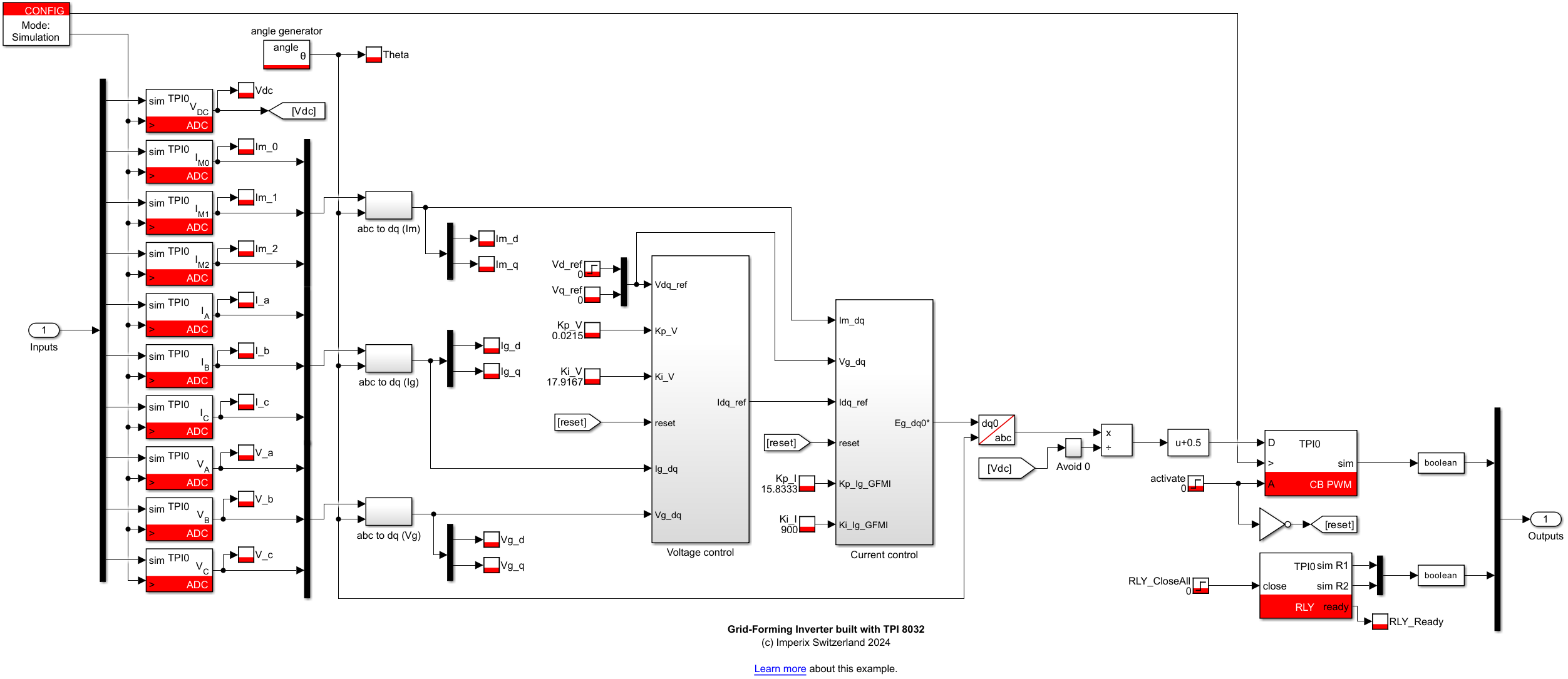
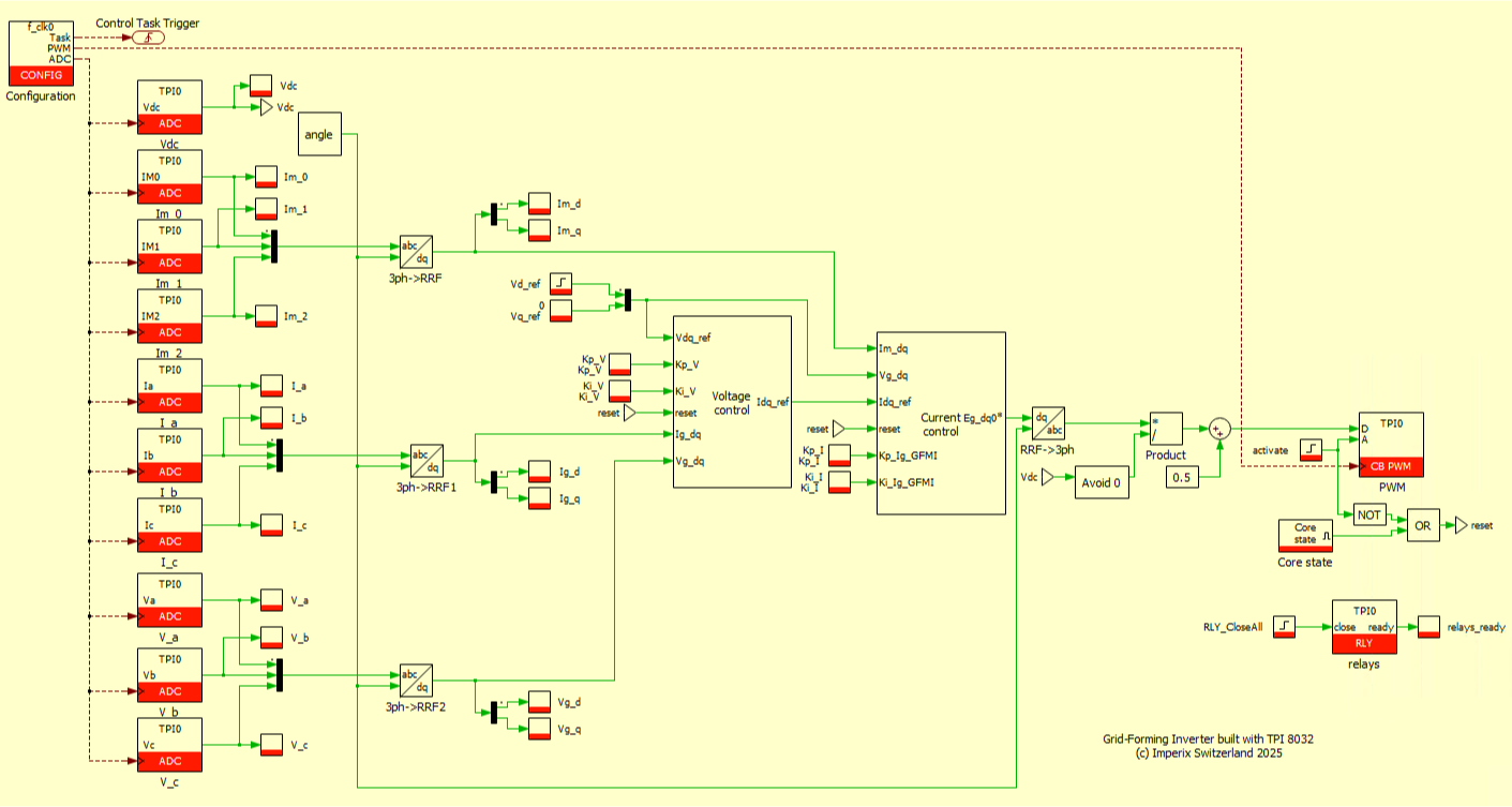
The control models available here after are implemented in Simulink and PLECS using the imperix ACG SDK blockset. The models can both simulate the system’s behavior offline and generate code for real-time execution on the TPI 8032 controller. To run these models, the minimum requirements are:
- Imperix ACG SDK 2024.2 or newer.
- MATLAB Simulink R2016a or newer.
- For simulation only: Simscape Electrical
- PLECS 4.5.9 or newer.
- TN168_Grid_Forming_Inverter includes the grid-forming inverter control with a single TPI connected to a passive load.
- TN168_GFMI_and_GFLI additionally includes a grid-following inverter connected to the AC terminals of the grid-forming inverter to perform load steps. This implementation requires two TPI 8032.
Experimental results
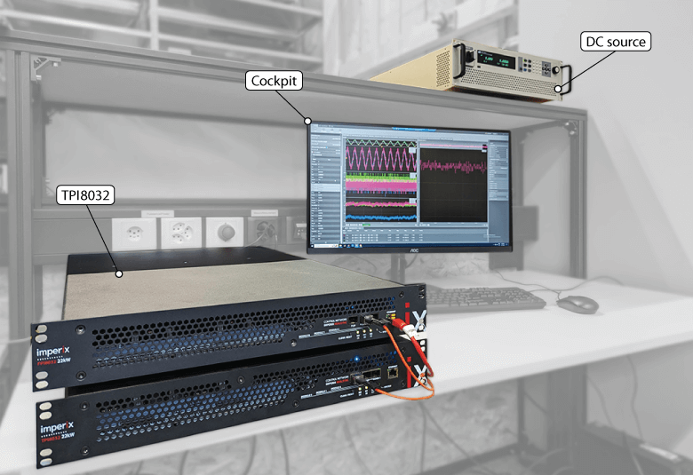
The experimental validation of the grid-forming control is carried out using two TPIs in a master-slave configuration, meaning they are programmed from the same Simulink/PLECS model. The GFMI is implemented on the master unit and connected via an SFP cable to the slave GFLI unit, which acts as an active load. Therefore, the required equipment is:
- 2x TPI 8032 three-phase inverter
- ACG SDK toolbox for automated generation of the controller code from Simulink or PLECS
- 1x DC power supply (800V)
- All the necessary cables
| Control and switching frequency | 50 kHz |
| DC bus voltage | 800 V |
| Desired grid voltage (L to N) | 230 V RMS |
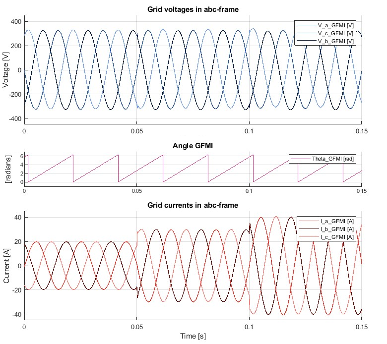
The dynamics of the GFMI are shown in the following figure. The GFLI applies different current steps:
- from 20 to 30A at t=50ms
- from 30 to 40A at t=100ms
The GFMI maintains the desired grid voltage of \(230V_{RMS}\) (blue curves) and alignment with the theta angle, regardless of the current steps imposed by the GFLI (red curves). This demonstrates the GFMI’s effectiveness in maintaining grid voltage amplitude and phase across different load conditions.
The following figure shows GFMI’s perturbation rejection capability in the dq frame. To challenge the control, a steep load step of -30A is applied at t=100ms.
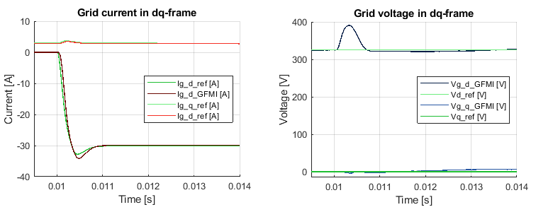
The change on the d-axis does not affect the q-component of the grid voltage, which is correctly decoupled from the d-component. In this example, the perturbation rejection on the d-axis is such that the resulting perturbation for a current step of 30A is 20%, which corresponds to 391V. The voltage recovers from the load step in approximately 1ms. The control requirements will determine whether the resulting performance, in terms of d-axis perturbance rejection, is acceptable. The tuning of the voltage and control loops can be adapted accordingly.
To go further…
The TPI 8032 is particularly suited for AC microgrid applications. The integrated AC precharge circuit simplifies the grid connection procedure. TN166 is a basic example illustrating the principle of grid-connected operation and the precautions for the precharge circuit. It is recommended to read this page first before running the TPI with the grid.
Furthermore, the TPI 8032 can be easily programmed to fit any purpose. More examples of TPI in microgrid applications are available in the knowledge base, such as:
- TN166: Active front end
- TN167: Grid-Following Inverter (GFLI)
- TN169: Proportional droop control
- TN170: Virtual synchronous generator for droop control
Moreover, the control strategy proposed in this article for the grid-forming inverter can also be applied to modern flexible smart grid applications, such as solid-state transformers (see AN015).
Academic references
[1] J. Rocabert, A. Luna, F. Blaabjerg and P. Rodríguez, “Control of Power Converters in AC Microgrids,” in IEEE Trans. on Power Electronics, Nov. 2012.
[2] D. B. Rathnayake et al., “Grid Forming Inverter Modeling, Control, and Applications,” in IEEE Access, Aug. 2021.
[3] H. Zhang, W. Xiang, W. Lin and J. Wen, “Grid Forming Converters in Renewable Energy Sources Dominated Power Grid: Control Strategy, Stability, Application, and Challenges,” in Journal of Modern Power Systems and Clean Energy, Nov. 2021.
[4] K.J. Åström and T. Hägglund, “PID Controllers: Theory, Design, and Tuning,” ISA, North Carolina, 1995.
 By Daniel Blardone • March 15, 2024 • TN169
 By Shu Wang • March 12, 2024 • TN171
 By Simon Strobl • March 11, 2024 • TN170