
Table of Contents
This note explains how to compute the discrete control delay of a control algorithm running on an imperix controller, and how to account for it in the controller tuning.
Context
The execution of a digital control algorithm inevitably introduces delays in the control chain. These delays are due not only to the algorithm’s execution time but also to external factors such as sensor and modulator delays. This overall delay affects the system response and therefore limits the achievable closed-loop control bandwidth. Knowledge of the total delay is therefore crucial for designing and tuning the controller to ensure stability and performance constraints.
For controller design, the various delays involved in the control loop are often lumped together into an equivalent total delay \(T_{d,tot}\) and modeled using a first-order approximation \(1/(1+sT_{d,tot})\). Based on this model, analytical tuning of the controller becomes possible, as further developed in PI controller implementation and illustrated in PI-based current control.
This note explains how to compute \(T_{d,tot}\) in the most common cases.
Definitions of the various delays
The total loop delay is the sum of all delays between the measurement of a state variable and the controller’s action on the plant. The different delays involved are defined below.
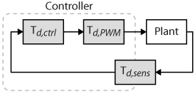
| Delay | Symbol | Definition |
|---|---|---|
| Sensing delay | \(T_{d,sens}\) | Delay in the measured quantity, due to finite sensor and analog chain bandwidth, and possibly filtering delay |
| Control delay | \(T_{d,ctrl}\) | Delay between sampling instant and duty-cycle update instant in the PWM modulator (FPGA peripheral) |
| Modulator delay | \(T_{d,PWM}\) | Average delay between duty-cycle update in the PWM modulator and resulting change in modulator output |
| Switching delay | \(T_{d,tran}\) | Delay between a change in the modulator output and the actual switching of the power device (can often be neglected) |
| Total loop delay | \(T_{d,tot}\) | Sum of the above delays, representing the total delay of the control system |
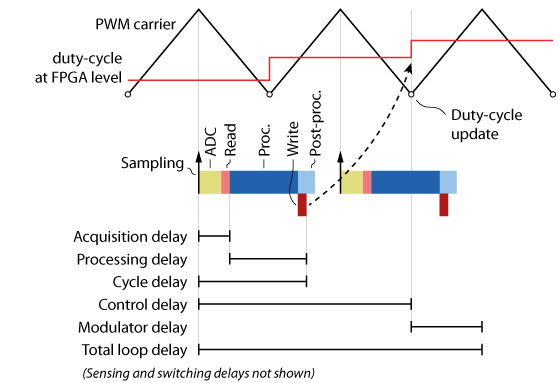
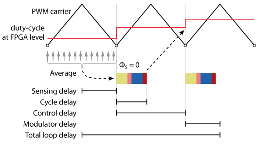
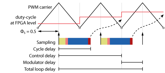
The figure below illustrates the different delays involved in a system using a triangular PWM carrier and implementing the single-rate update of the duty cycle (at the bottom of the carrier).
Sensing delay
The sensing delay \(T_{d,sens}\) includes the sensor delays, plus those inherent to the controller’s analog front-end:
- The sensor delay depends on its bandwidth \(f_{bw}\) and filter order. If no value is specified, the delay can typically be assumed to be between \(1/(2\pi f_{bw})\) and \(2/(2\pi f_{bw})\).
- In the controller, the delay introduced by the analog front-end is generally comparatively low, as imperix controllers feature high analog bandwidth. However, delays may require consideration if:
- Synchronous averaging is used: the induced group delay is equal to half the averaging period (typically half a control period).
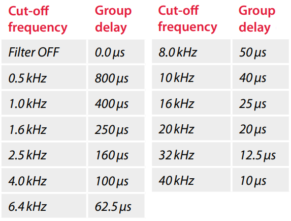
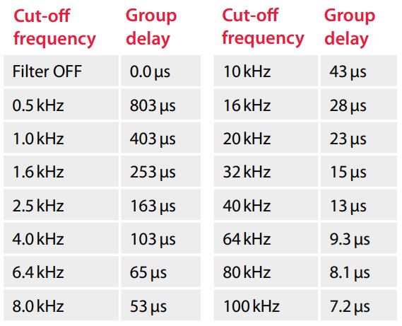
- A low-pass filter is used (B-Box 3 and B-Box 4 only): the induced delay depends on the selected cutoff frequency (see tables below).
- A high-bandwidth sensor is used: in this case, the controller’s analog bandwidth may no longer be high relative to the sensor.
Control delay
The control delay \(T_{d,ctrl}\) is defined as the elapsed time between the sampling instant and the duty-cycle update in the PWM modulator. Due to the discrete nature of the control process, this delay typically takes values that are fractions or multiples of the control period Ts, such as 0.5Ts, Ts, or 1.5Ts, depending on the relative timing between ADC sampling and the corresponding PWM register update.
Imperix controllers are architected to minimize this delay, notably by implementing a rigorously unpipelined data path. More information about their firmware architecture is provided in PN253. The article details the various components of this delay, which are summarized below and are also visible in Cockpit’s Timings tab.
| Delay | Symbol | Definition |
|---|---|---|
| Acquisition delay | \(T_{acq}\) | Delay between sampling and data availability in the CPU. = ADC conversion time (ADC) + FPGA-to-CPU transfer time (Read) |
| Processing delay | \(T_{pr}\) | CPU processing time (Proc.) |
| Write delay | \(T_{wr}\) | CPU-to-FPGA transfer time (Write) |
| Cycle delay | \(T_{cy}\) | Delay between sampling instant and newly computed data available in FPGA (\(T_{cy}=T_{acq}+T_{pr}+T_{wr}\), see dedicated section below) |
Acquisition delay
The acquisition delay is the time between the sampling instant and the moment the resulting value becomes available to the CPU. It consists of the ADC conversion time, plus the transfer time from the ADC to the CPU, possibly over the control network:
- The ADC conversion time depends on the controller type, as listed in the table below:
| Device | ADC conversion time |
| B-Box 4 | 0.2 µs |
| B-Box RCP | 2 µs |
| B-Box Micro | 0.5 µs |
| B-Board PRO | 0.5 µs |
| TPI 8032 | 0.5 µs |
- The data transfer time is comparatively short (in the tens of ns) and depends mainly on the number of ADC channels being read. This delay can be observed in Copckpit’s Timings tab.
Processing delay
The processing depends mainly on the complexity of the executed control algorithm and is thus application-dependent. Although it is constant and deterministic, it cannot be anticipated from Simulink or PLECS. As such, it must be measured at runtime, via the Timings tab. For example, the control of the PV boost and three-phase grid-tied inverter (AN006) gives the following figures:
- Cycle delay (total) \(T_{cy}\): 6 µs
- Acquisition delay \(T_{acq}\): 2.072 µs (includes 2 µs ADC delay in B-Box RCP)
- Processing delay \(T_{pr}\): 3.9 µs
- Write delay \(T_{wr}\): 0.1 µs
Modulator delay
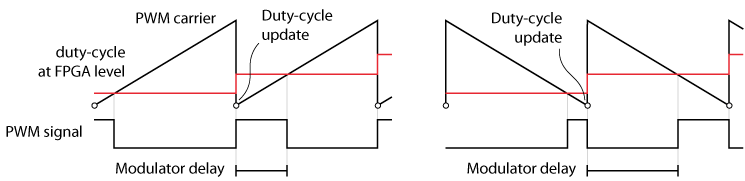
Most previously defined delays are straightforward and hardware-dependent. However, the modulator delay requires further clarification, as it varies according to the PWM peripheral parameters. Technically, this delay represents the time between the instant a new duty cycle is registered and the instant it is reflected in the PWM output pulse. Since this duration varies with the duty cycle, a statistical average is typically used.
Sawtooth carrier
The sawtooth carrier introduces a delay that depends on the duty-cycle \(d\) and the switching period \(T_{sw}\). From the figure below, it can be deduced that this delay is:
- Sawtooth carrier: \(T_{d,\text{PWM}}=dT_{sw}\)
- Inverted sawtooth carrier: \(T_{d,\text{PWM}}=(1-d)T_{sw}\)
For controller tuning, the average value \(T_{d,\text{PWM}}=T_{sw}/2\) is generally used, for both sawtooth carrier shapes.
Triangular carrier
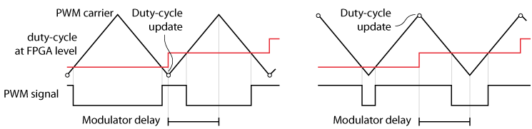
The modulator delay calculation is more complex since both rising and falling edges of the PWM signal are affected by the duty-cycle value. A small-signal approximation introduced in [1] and further developed in [2] shows that \(T_{d,\text{PWM}}=T_{sw}/2\) for single-rate update.
Intuitively, the duty-cycle update has an effect on two PWM edges: before and after the carrier midpoint, resulting, on average, in an effect after half a switching period [1]. This also means the delay is identical for triangular and inverted-triangular carriers.
With double-rate update, the modulator delay is reduced to \(T_{d,\text{PWM}}=T_{sw}/4\) [1], provided that the sampling is also performed at double rate (double-rate sampling, \(T_s=T_{sw}/2\)).
Direct output PWM
If no PWM modulator is used (e.g. when using the DO-PWM module), the modulator delay is \(T_{d,\text{PWM}}=0\). In this case, the firing signal is updated as soon as a new value is available in the FPGA, meaning that \(T_{d,ctrl}=T_{cy}\).
Examples
Single-rate update with synchronous averaging
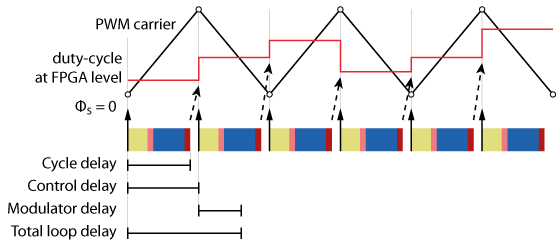
Let us consider the following configuration, which is the default configuration with imperix controllers:
- The switching and sampling periods are the same \(T_{sw}=T_{s}\).
- The sampling phase is \(\phi_{s}=0\), which also defines when the interrupt is triggered.
- All ADC channels use synchronous averaging.
- The PWM modulator uses a triangular carrier with a phase of zero and single-rate update (i.e. update at the bottom of the carrier).
- The current sensor bandwidth is 200 kHz.
In this case, the total loop delay is computed as follows:
- Sensing delay: \(T_{d,sens}= T_s/2\) (due to averaging)
- Control delay: \(T_{d,ctrl} = T_s\)
- Modulator delay: \(T_{d,\text{PWM}}=T_{sw}/2\) (triangular carrier)
- Switching delay: neglected, sub-microsecond
- Total loop delay: \(T_{d,tot}=T_{d,sens}+T_{d,ctrl}+T_{d,\text{PWM}}=2T_s\)
Single-rate update with synchronous sampling
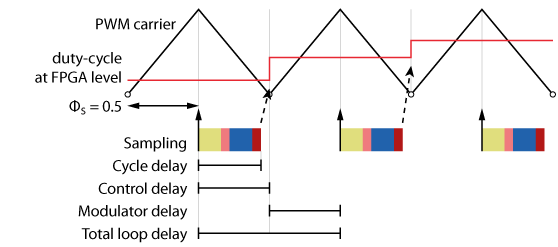
Let us consider the following standard configuration:
- The switching and sampling periods are the same \(T_{sw}=T_{s}\).
- The sampling phase is \(\phi_{s}=0.5\) to ensure sampling in the middle of the current ripples.
- The PWM modulator uses a triangular carrier with a phase of zero and single-rate update (i.e. update at the bottom of the carrier).
- The current sensor bandwidth is 200 kHz.
In this case, the total loop delay is computed as follows:
- Sensing delay: neglected (\(\approx 800\,\text{ns}\))
- Control delay: \(T_{d,ctrl} = 0.5T_s\)
- Modulator delay: \(T_{d,\text{PWM}}=T_{sw}/2\) (triangular carrier)
- Switching delay: neglected, sub-microsecond
- Total loop delay: \(T_{d,tot}=T_{d,ctrl}+T_{d,\text{PWM}}=T_s\)
Regular control algorithm
In this first case, we assume that the control algorithm can be executed fast enough, so that the cycle delay is shorter than half a control period (\(T_{cy} < 0.5T_s\)). This is the case for most control implementations running on imperix controllers.
In this case, the total loop delay is computed as follows:
- Sensing delay: neglected (\(\approx 800\,\text{ns}\))
- Control delay: \(T_{d,ctrl} = T_s/2\)
- Modulator delay: \(T_{d,\text{PWM}}=T_{sw}/2\) (triangular carrier)
- Switching delay: neglected, sub-microsecond
- Total loop delay: \(T_{d,tot}=T_{d,ctrl}+T_{d,\text{PWM}}=T_s\)
Heavy control algorithm
Now let’s assume that the control algorithm is heavy and the cycle delay is longer than half a control period (\(T_{cy} \geq 0.5T_s\)).
In this case, the total loop delay is computed as follows:
- Sensing delay: neglected (\(\approx 800\,\text{ns}\))
- Control delay: \(T_{d,ctrl} = 1.5T_s\)
- Modulator delay: \(T_{d,\text{PWM}}=T_{sw}/2\) (triangular carrier)
- Switching delay: neglected, sub-microsecond
- Total loop delay: \(T_{d,tot}=T_{d,ctrl}+T_{d,\text{PWM}}=2T_s\)
General case
With single-rate update and triangular carrier, the total loop delay can take two values:
- If \(T_{cy} < (1-\phi_s)T_s\), \(T_{d,ctrl} = (1-\phi_s)T_s\) and \(T_{d,tot}=(1.5-\phi_s)T_s \)
- If \(T_{cy} \geq (1-\phi_s)T_s\), \(T_{d,ctrl} = (2-\phi_s)T_s\) and \(T_{d,tot}=(2.5-\phi_s)T_s\)
These results suggest that the smaller the sampling phase, the smaller the delay. However, the choice of the sampling phase should also rely on current ripple sampling considerations. Generally speaking, the choice of the sampling phase is a trade-off between control bandwidth and the control accuracy.
Double-rate update with synchronous sampling
Now, let us consider the following configuration:
- The switching and sampling periods are \(T_{sw}=2T_{s}\) (double-rate sampling).
- The sampling phase is \(\phi_{s}=0\).
- The PWM modulator uses a triangular carrier with a phase of zero and double-rate update (update at the top and bottom of the carrier).
- The current sensor bandwidth is 200 kHz.
In this case, the total loop delay does not depend on the execution time of the algorithm, unlike with single-rate update. It is computed as follows:
- Sensing delay: neglected (\(\approx 800\,\text{ns}\))
- Control delay: \(T_{d,ctrl}=T_s\)
- Modulator delay: \(T_{d,\text{PWM}}=T_{sw}/4=T_s/2\) (triangular carrier with double-rate update)
- Switching delay: neglected, sub-microsecond
- Total loop delay: \(T_{d,tot}=T_{d,ctrl}+T_{d,\text{PWM}}=1.5T_s\)
References
[1] D. M. Van de Sype, K. De Gusseme, A. P. Van den Bossche and J. A. Melkebeek, “Small-signal Laplace-domain analysis of uniformly-sampled pulse-width modulators,” 2004 IEEE 35th Annual Power Electronics Specialists Conference, Aachen, Germany, 2004, pp. 4292-4298 Vol.6.
[2] S. Buso and P. Mattavelli, “Digital Control in Power Electronics”, 2006.
 By Benoît Steinmann • April 2, 2021 • SD010
 By Jonathan Orsinger • March 30, 2021 • AN006