
Table of Contents
Imperix controllers rely on an internal architecture and operating principles that sometimes differ significantly from those of traditional DSPs, MCUs, and general-purpose HIL/RCP systems.
Because these unique characteristics are exactly what sets imperix apart, understanding them is often essential to fully leveraging their capabilities. To that end, this article explores the main particularities of the controllers and presents their key operating principles.
Overview of imperix controllers
Architecture overview
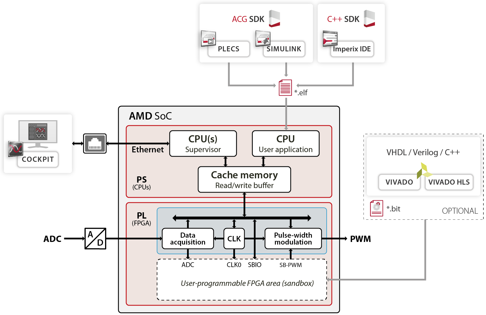
Imperix controllers are based on AMD System-on-Chip (SoC) devices. This allows for an effective separation of the digital signal processing tasks among two different types of resources:
- The processing system (PS) leverages fast CPU cores to perform floating-point arithmetic operations quickly. Imperix controllers, being multi-core systems, have one core dedicated to user-defined control code, while the other cores handle system monitoring and data logging.
- The programmable logic (PL) area is used to implement specialized functions at the hardware level (e.g., FPGAs), with absolute determinism and very high temporal resolution. This notably concerns pulse-width modulators (PWM), I/O peripheral drivers, etc.
Thanks to the CPUs and FPGA sharing the same die, an extremely low data transfer latency between them is achieved. This more than compensates for the lower CPU clock speed when compared to the x86 architecture.
More information on the architecture and its benefits is given in PN253.
CPU programming (PS side)
On the PS side, only one core is user-programmable, referred to as the user application CPU. In parallel, other cores host a Linux-based supervisor that comes as a pre-defined embedded environment. For programming the user application CPU, two approaches are possible:
- Model-based graphical programming: typically, the control algorithms are developed in Simulink or PLECS, and then automatically translated into executable user code. This approach is supported by the ACG SDK.
- Programming in C/C++ code: alternatively, the controllers can be programmed “manually” using the C/C++ Software Development Kit (CPP SDK).
Instructions for getting started with the software development environments are given in:
FPGA programming (PL side)
The PL side is also user-programmable, with most of the logic resources available for that.
This opens a door granting maximum flexibility or performance to advanced users. Programming the FPGA is, however, only rarely truly required, as imperix controllers already present exceptional closed-loop control performance from the CPU.
For those interested in leveraging these resources, the minimum required imperix firmware is available as a pre-packaged IP block that only needs to be instantiated in a custom-created bitfile. Getting-started information for programming the FPGA is given in PN159.
Program upload and real-time monitoring
Regardless of the development environment, the compilation generates an executable (.elf) corresponding to the user code (for the user application CPU). This executable is ultimately uploaded onto the controller via Cockpit (over Ethernet), and is generally launched immediately afterward.
A custom bitfile (.bit) implementing customized FPGA logic (PL side) can also be uploaded onto the controller. This file is then written on the SD card and loaded at the next startup.
For the supervisor CPU(s), the corresponding Linux resources reside permanently on the SD card and are automatically loaded at startup. This is part of the on-device firmware, which can be updated through the regular releases of the imperix SDKs.
PN138 provides guidance on how to program imperix controllers and monitor them during runtime.
Real-time control execution
Base system startup and hardware initialization
Once powered up, imperix controllers execute the following sequence of tasks:
- The supervisor CPU (Linux) is started first. It identifies the supporting hardware, loads the initial FPGA configuration, runs network discovery (RealSync, see PN264), and enables Ethernet communication. If the user has stored a custom bitstream, the corresponding FPGA configuration is loaded instead of the default one. During this time, a “booting in progress” status is displayed on the LCD screen (B-Box 3 and 4).
- Once the boot process is finished, the controller is technically ready to use. However, user code is often not present yet, as it is only loaded afterward via Cockpit. At this point, a “code stopped, PWM disabled” message is displayed on the LCD screen.
- Alternatively to 2., if the user has configured the controller to automatically start user code at boot time (see Cockpit’s user guide), this code is launched immediately (see next section).
During that time, all physical PWM lanes (optical and electrical) are forcedly maintained low by the safety FPGA (or external hardware logic in gen. 3 devices). This way, imperix controllers ensure that no dangerous 1:1 state can occur during startup, shutdown, or reprogramming.
User code launch
The initialization phase should be clearly distinguished from the running phase. During initialization, the following actions take place:
- Since a user code is desired to be launched, the controller self-identifies as a master device. This is trivial in a setup with only one controller, but has multiple consequences in master-slave or multi-master configurations (see PN264).
- Before the user code is truly launched, a cryptographic process is executed to check that a valid license is present (see imperix licensing policy).
- The clock- and timer-dependent configurations are set, including the base configuration for the CLK and ADC peripherals and the main CPU interrupt.
- The user-specific configuration is set, notably containing a variable number of ADC and PWM resources. This is when the validity of the user configuration is checked (existence of the desired hardware resource, potential addressing conflicts, out-of-range settings, etc.). If problems arise, warnings and errors are thrown and displayed in Cockpit’s log messages.
- High-level, user-specific initialization actions are taken. When working in C/C++, this is when the
UserInit()method is called. When working with Simulink/PLECS, this is whenSimulinkInitialize()is called. - Finally, the CPU interrupt and watchdog are enabled. At this point, a “code running, PWM disabled” message is displayed on the LCD screen.
From this point onward, the user code is considered to be running safely. Thanks to that, the safety FPGA authorizes the user app CPU to enable the PWM outputs when desired (either manually in Cockpit or via a function call in the code).
Interrupt-based operation
The user code uses a hardware interrupt to schedule the execution of the control algorithms and manage associated read/write accesses to/from FPGA-based peripherals. This is a hard real-time task, because no overrun is allowed (a protection trip occurs otherwise, see below).
Inside imperix controllers, the user app CPU interrupt is also rigorously timed, following a strictly unbuffered pipeline, meaning there is no cycle delay between sampling and processing, nor between processing and the PWM update.
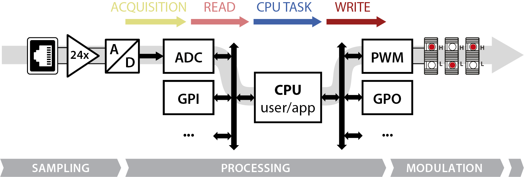
Overall, the processing of the main interrupt follows a 4-step sequence:
- Acquisition: ADC data are retrieved and processed (filtered, downsampled, etc.) inside the FPGA.
- Read: once the acquisition finishes, these data are transferred from the FPGA to the shared memory, along with data from other input peripherals (GPI, DEC, etc.).
- CPU control task: the user app CPU reads the input data from the shared memory, executes the user-defined control algorithm and writes the output data back inside the shared memory. When working in C/C++, this is when the
UserInterrupt()method is called. When working with Simulink/PLECS, this is whenSimulinkStep()is called. - Write: at the end of the CPU task, the newly calculated parameters are transferred back from shared memory to the FPGA peripherals (PWM, GPO, etc.).
- Simultaneously with the Write phase, the CPU also writes a second data set to the shared memory, refreshing the variables the user wishes to monitor (probes and tunable parameters).
PWM parameters (e.g., duty cycle and phase) are always transferred immediately after the CPU task. However, they are latched at configurable instants related to the PWM operation rather than the end of the write sequence. In fact, although these instants are generally synchronized with the control execution, this is not always the case (e.g. variable-frequency operation).
The illustration below shows how these steps occur in a single-controller configuration. In a master-slave configuration (see PN264), the acquisition is triggered simultaneously and runs in parallel on all devices. Only the durations of the read and write phases are slightly extended due to the higher amounts of data exchanged.
The above-described process defines two different and equally important timing sets:
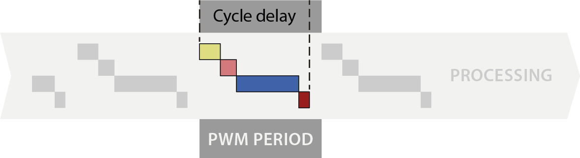
The total control cycle delay
This represents the total time elapsed from the analog sampling instant to the FPGA’s PWM parameter update. It is made of:
- ADC acquisition delay: the time required to physically sample and process the analog data. This can be as low as 200 ns inside the B-Box 4.
- CPU control task execution: This is the effective computation time required by the implemented control algorithms.
- Read and write delays: These represent the CPU-to-FPGA data transfer times. These are generally negligible, except in large multi-device configurations.
The total CPU load
This represents the total workload for the user app CPU. It is independent of the I/O data transfers, but encompasses:
- CPU control task execution: This is the effective computation time required by the implemented control algorithms.
- CPU data monitoring: This represents the time required for the user app CPU to write the monitored data to the shared memory (oversampled data are excluded from this).
The total CPU load is what generally constrains the maximum execution rate for a given code. This cannot exceed 100% (a real-time violation occurs otherwise, see below).
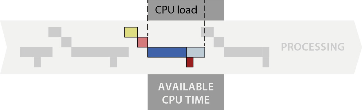
Cockpit provides a clear representation of these performance metrics within the Timings info tab.
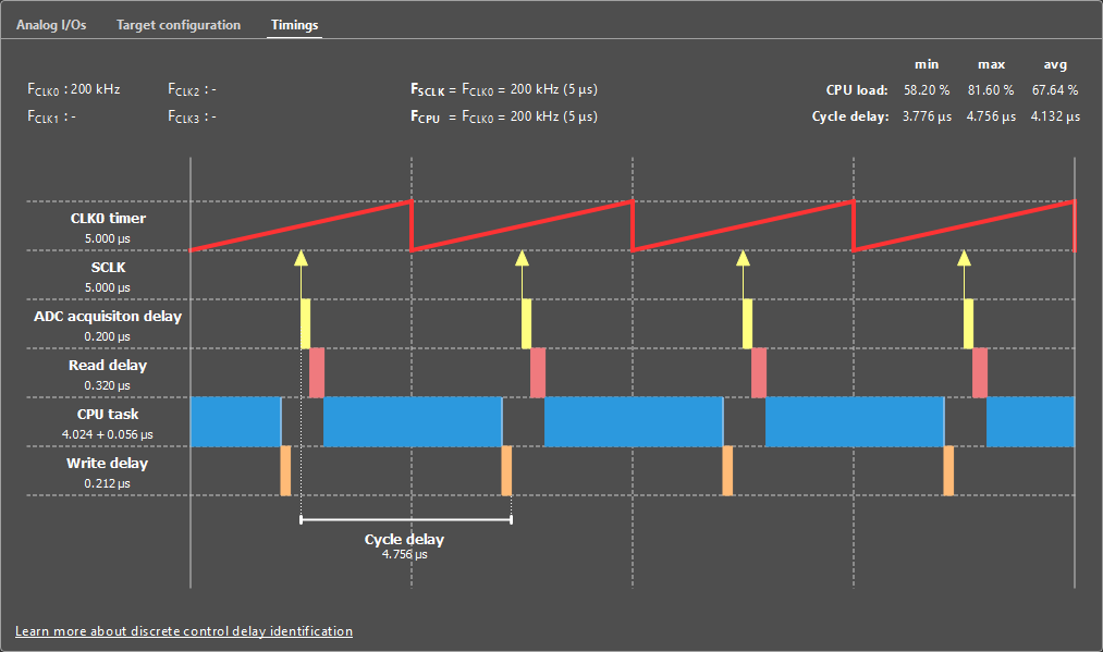
Understanding the total control cycle delay is critical for optimizing the bandwidth and phase margin of closed-loop control algorithms. On imperix controllers, this delay is rigorously constant (extremely low jitter) and heavily minimized. However, the exact duration of each task depends on the complexity of the user code and is hence unknown before execution. Therefore, the optimization of the controller typically follows an iterative workflow: users must first load the initial control code onto the controller, read the cycle delay from the Timings window, and then tune the controller parameters based on the actual cycle delay. More information on that topic is given in PN142.
On the other hand, the total CPU load is always what constrains the maximum achievable CPU execution rate. This essentially depends on the complexity of the implemented control algorithms (control task execution, dark blue in Cockpit’s Timings diagram), but marginally also on the number of monitored variables (data monitoring, light blue in the Timings diagram), especially from light, but very fast applications (typically above 300-400kHz).
Background operations
When not serving the main interrupt, the user app CPU has essentially nothing time-critical to do. It then executes background functions, including the following tasks:
- Exchanging non-deterministic data with the supervisor, such as communication data carried using Ethernet, CAN, Modbus, etc.
- Refreshing OPC-UA variables and transmitting log messages.
- Servicing the CPU watchdog.
- Executing user-defined actions in
UserBackground()(C/C++ only). - Executing non-critical control tasks defined through software interrupts. For example, an MPPT algorithm can be executed at a slower rate than the main CPU (see PN145 and PN155).
In the background, hard real-time execution of the code cannot be guaranteed, especially under high CPU loads. Because of that, the UserBackground() and software interrupts should only be used for tasks that are significantly slower than the main interrupt.
Timers and interrupt generation
Most microcontrollers fundamentally base their timings on the pulse-width modulators (PWM). Typically, an ADC sampling interrupt is generated in the middle of the PWM period, whereas the CPU interrupt is generated by an end-of-conversion flag after the ADC conversion.
While intuitive, this approach is incompatible with distributed control and modulation because it inevitably introduces undesirable latency. Instead, imperix controllers base their timing on independent clocks and use predetermined relative phase shifts for each FPGA-based peripheral (more about this in PN259).
In practice, four synchronized time bases are available, implemented through CLK0-CLK3.
- CLK0 is special as it is used for all the sampling- and processing-related events. Its frequency must, however, be constant (regular sampling).
- CLK1-CLK3 are additional clocks that can be used for PWM operation. These can be of variable frequency.
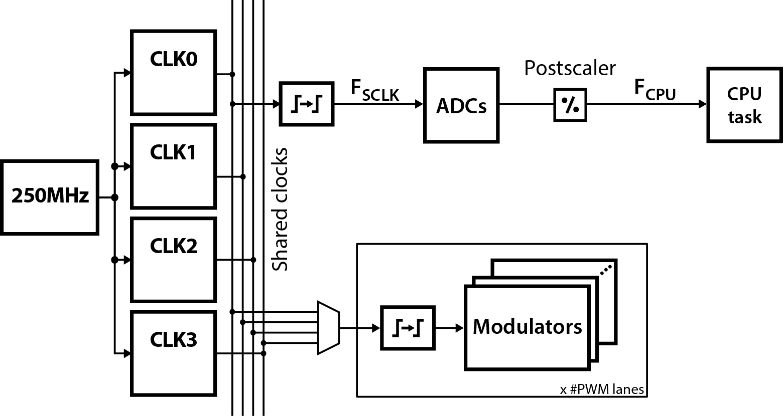
Thanks to imperix’s RealSync technology, these clocks are natively distributed across the control network, enabling precise, transparent, and synchronous timing of all events among stacked controllers (more on this in PN264).
This approach yields perfectly equivalent capabilities while strongly minimizing latencies. Furthermore, synchronous oversampling and synchronous averaging techniques can be easily implemented. As a result, imperix controllers support all standard sampling configurations, as well as additional attractive, more advanced options, which are described in the following sections.
Sampling configuration
In power electronics, sampling is commonly arranged to be synchronous with the modulation, with a finely controlled relative phase. This way, aliasing can be advantageously leveraged to extract information about the sliding-average value of a measured quantity without prior low-pass filtering (and its associated group delay).
In contrast to general-purpose RCP systems, this approach is natively supported by all imperix controllers. The corresponding single- and double-update rate configurations are illustrated below and further documented in PN259.
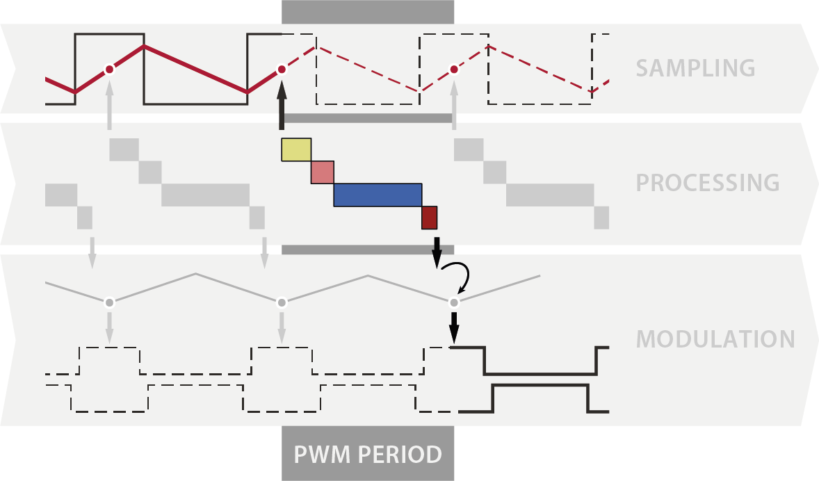 Synchronous sampling with single update rate
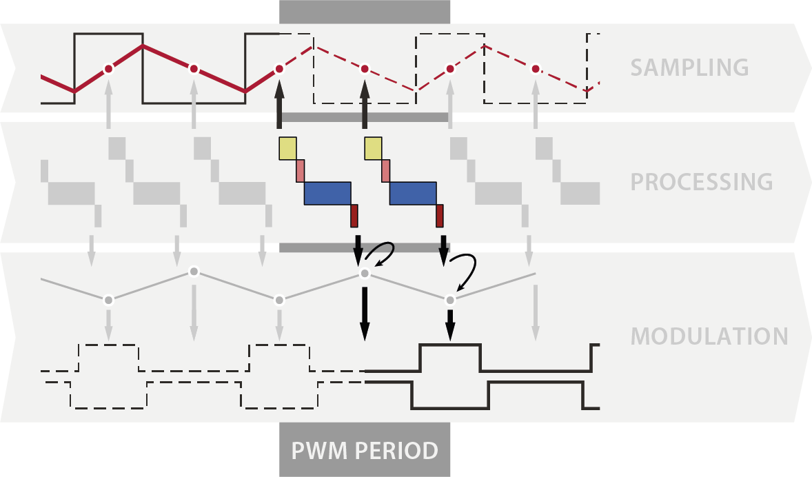 Synchronous sampling with double update rate
Apart from these two basic configurations, B-Box controllers also support two other options:
- Anti-alias filtering prior to ADC sampling (with configurable low-pass filters).
- Synchronous averaging.
These two techniques are described in more detail in PN258. Notably, synchronous averaging is extremely valuable for rejecting a wide range of perturbations when synchronous sampling fails to yield an accurate estimate of the average value. (In other words, in all cases where the sampled signal is anything other than a perfectly triangular waveform. More details on that are also given in PN258.)
PWM configuration
On the modulation side, imperix controllers offer six types of pre-implemented, fully pre-validated pulse-width modulators. The related documentation is available in SD009.
At the hardware level, these modulators share the following key features:
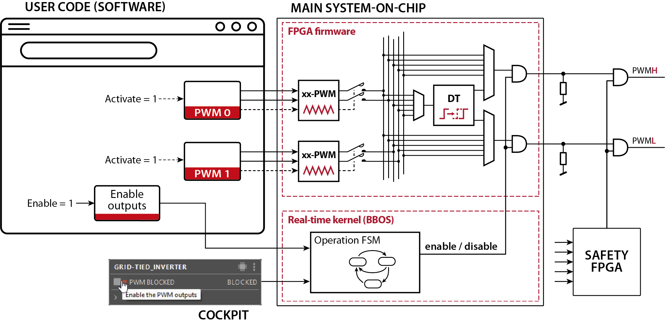
- Output mode: PWM outputs can be configured as individual lanes (one bit) or a full channel (two bits) with a configurable dead time. When operated as a channel, outputs are guaranteed to never produce the dangerous “1:1” state by design, because this state is made physically impossible to generate from within the FPGA logic.
- Protection & global enable: PWM outputs are globally controlled by the core state and are immediately shut down in the event of a fault (see “software-independent protections” below).
- Channel-wise activation: Independent activation is possible per channel using the activate pin. This permits selective energization of only one part of the application (e.g., one inverter in a complete back-to-back configuration) once the PWM enable action is triggered.
Hardware and analog front-end configuration
B-Boxes 3 and 4 feature a high-performance analog front-end (high bandwidth, high CMRR, high precision) that is fully configurable. This grants users the flexibility to adapt to a broad range of sensors while ensuring excellent signal integrity in challenging EMI environments.
Additionally, all controllers -except the B-Board PRO- possess hardware protections that operate by instantly blocking the PWM outputs in case of an over-value (see below). A key feature of imperix controllers is that these protections operate fully independently from the user code and FPGA logic.
Due to the independent nature of this analog front-end, its configuration is part of the hardware rather than the user code and is carried along with it. On B-Box units, the corresponding parameters can also be set directly from the front panel (screen and button). For other devices, the available approaches are summarized below:
| F.-E. configuration | Config. save/restore | Documentation | |
|---|---|---|---|
| B-Box 4 | Front panel or Cockpit | Cockpit | PN252 |
| B-Box 3 (RCP) | Front panel only | USB key | PN105 |
| B-Box micro | Cockpit only | Cockpit | PN106 |
| B-Board 3 (PRO) | N/A | N/A | N/A |
| TPI8032 | N/A | N/A | N/A |
Core operating states
Imperix controllers block their outputs when inappropriate operation occurs, caused by controller misbehavior, unexpected events, or excessive operating conditions (current, voltage, temperature, etc.). Various trip sources are supported to cover all potential fault scenarios in a real application. This is further documented in PN263.
When a protection trip is triggered, hardware protections instantly block all PWM outputs, thereby preventing any damage to the power stage. Immediately after, various indicators and log messages are available to help identify the root cause and facilitate troubleshooting. This is also further documented in PN263.
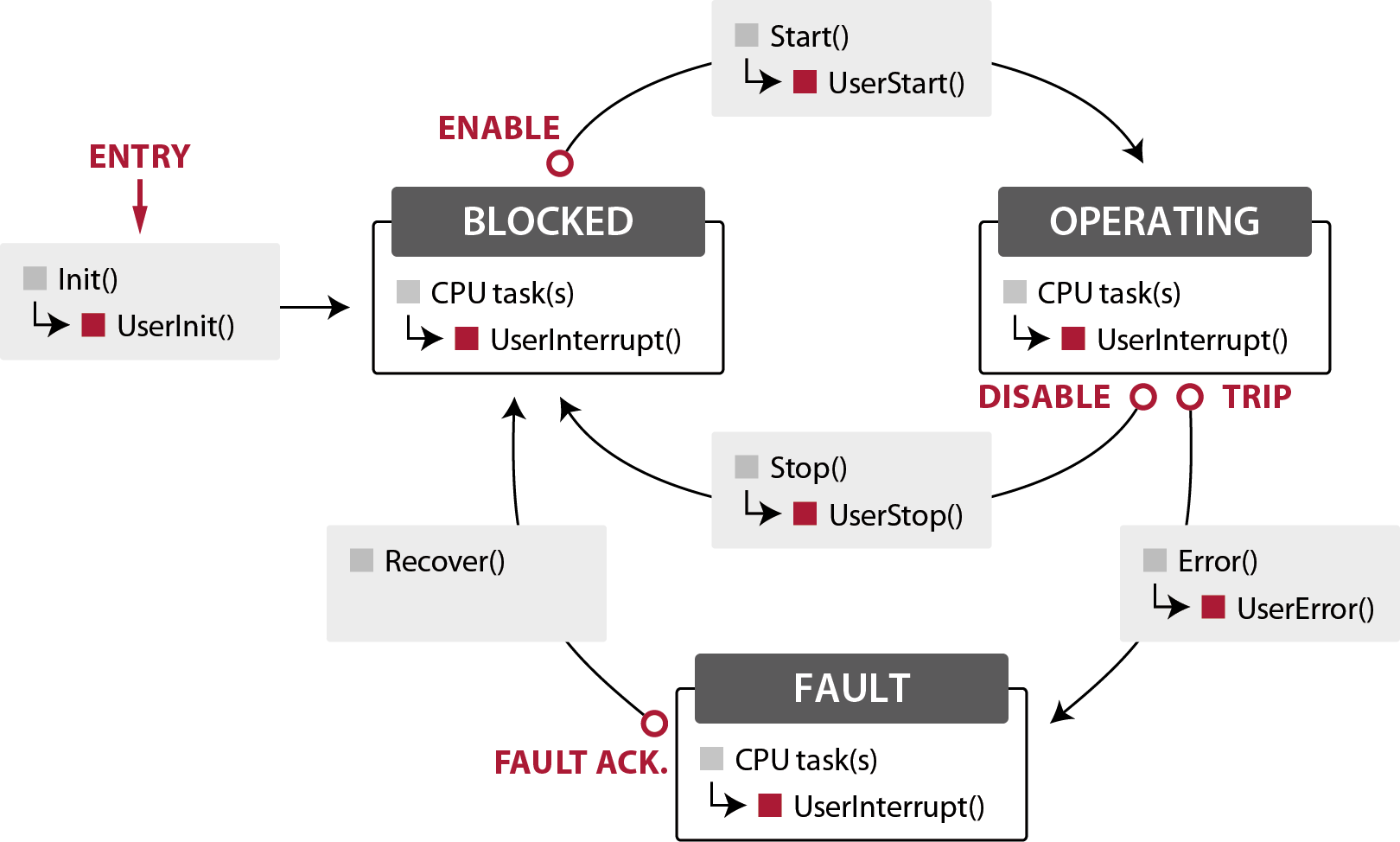
At the software level, these mechanisms are supported by a dedicated state machine implementing three core states in relation to the power stage:
- FAULT: An error occurred, and the system is awaiting acknowledgment. All PWM outputs are blocked similarly to the BLOCKED state.
- BLOCKED: The controller is operating normally, but all PWM outputs are inhibited. The CPU control task is hence running (including all the contained control algorithms and communication functions), but the power stage remains blocked.
- OPERATING: The controller is operating normally and all PWM outputs are normally produced. The power stage is actively driven.
The illustration below shows the sequence of events associated to an over-current. This is detailed in PN263.
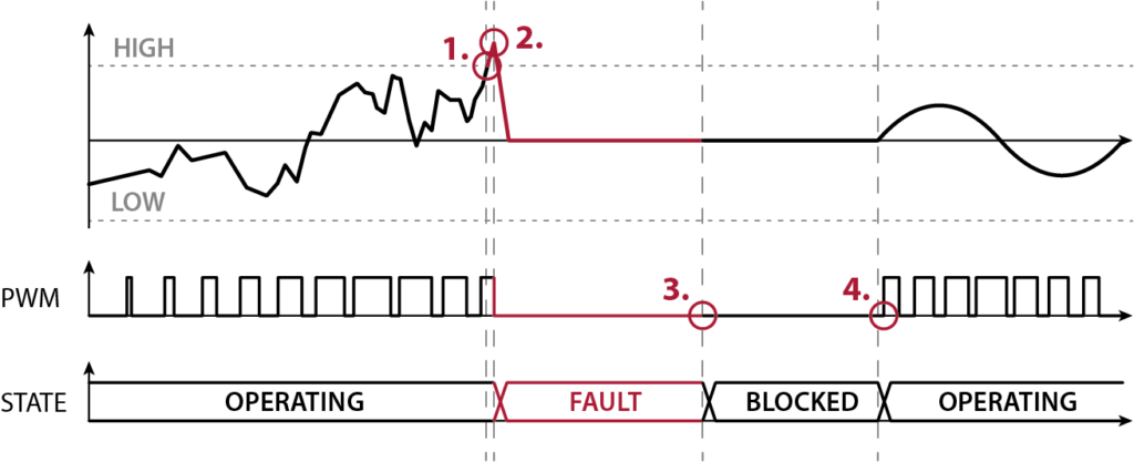
Legend:
- Threshold exceeded
- All PWMs blocked
- User acknowledgement
- Operation resumed
Importantly, the core states shall not be confused with application-level operating states, i.e., those corresponding to the whole power converter. For instance, operating states such as CHARGING, SYNCHRONIZING, and DICHARGING (or similar) all require the converter to actually be switching. As such, they are typically “contained” within the OPERATING core state and managed by a secondary, application-level, state machine instead.
State transitions
PWM enable
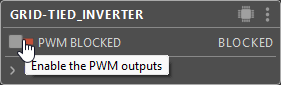
This transition, from BLOCKED to OPERATING, is generally triggered manually in Cockpit by clicking the associated button, available for each project. Alternatively, PWM outputs can be enabled programmatically via the enable PWM outputs block or the CoreStart() function.

PWM disable
Reciprocally, the transition from OPERATING to BLOCKED, disabling all PWM outputs, can be triggered by clicking the same button in Cockpit, or by forcing the enable PWM outputs block to zero. For C/C++ users, the CoreStop() function also achieves this result.
Protection trip
Various fault types (detailed in PN263) are supported. When a fault is triggered, hardware protections instantly block all PWM modules and set the CORE state to FAULT. A message is then displayed in Cockpit to indicate the trip source and guide the subsequent troubleshooting steps.
Importantly, upon entering the FAULT state, PWM channels are automatically disabled, whereas GPO channels typically remain operational. This is the main difference between these two output types. To automatically force a GPO pin to ‘0’ during a fault (e.g., to open a relay), a special check box must be ticked in the GPO block mask (ACG) or a special configuration function must be called during initialization (CPP). More details are given in PN006.
Trip acknowledgement
In power electronics, a protection trip often indicates a critical underlying issue or insufficient control stability. In such cases, restarting the operation immediately without investigation may cause catastrophic damage. Therefore, imperix controllers require an explicit trip acknowledgment step for analog overvalues (e.g., over-current or over-voltage). Other fault types clear immediately once the faulty condition disappears (auto-acknowledgment); some don’t. The complete list of fault types is given in PN263.
Visual representations of the core state
The core state can be observed via the core/sys front panel LED, the LCD screen (on B-Boxes), or the Cockpit.
| Core state | No code running | BLOCKED | OPERATING | FAULT |
|---|---|---|---|---|
| Cockpit | 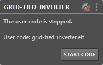 | 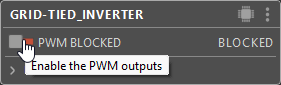 | 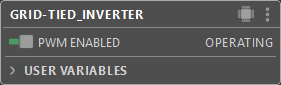 | 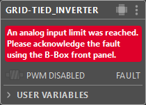 |
| B-Box 4 | 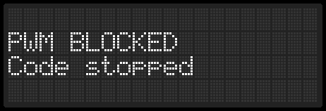  | 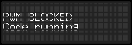  | 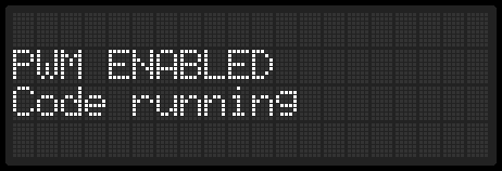  | 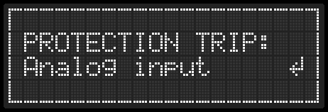  |
| B-Box 3 (RCP) | 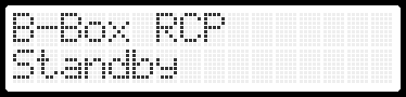  | 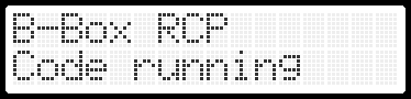  | 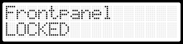  | 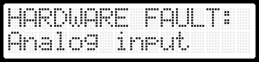  |
| B-Board PRO |  |  |  |  |
| TPI8032 |  |  |  |  |
| B-Box Micro | N/A | N/A | N/A | N/A |
To go further
When seeking to understand how imperix controllers operate, the following articles may provide valuable insight:
- PN253 presents the architecture of imperix controllers, which is further detailed in PN260 for the acquisition side and in PN262 for the modulation side.
- PN263 explains how hardware protections operate. Practical advice on configuring the protection thresholds is addressed in PN257.
- PN264 is somewhat an extension of this page, specific to multi-controller systems (stacked operation).
When seeking to get started with imperix controllers, the following articles might help:
Related Articles
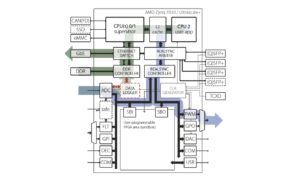
Architecture of imperix controllers

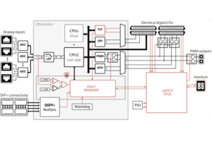
Hardware protections on imperix controllers

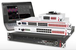
Programming and operating imperix controllers

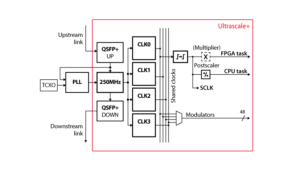
Timing configuration on imperix controllers
