Table of Contents
This note provides in-depth guidance for accurately and efficiently simulating an imperix controller and its associated plant using the ACG SDK in PLECS. Because the underlying mechanisms are identical to those used in real-time operation, this content is also valuable for understanding the controller’s behavior during real-time execution.
Recommended articles related to the ACG workflow are shown below. A series of video tutorials is also available with similar content, illustrating the Simulink workflow.
| Step | Documentation | Videos | |
|---|---|---|---|
| 1. Software installation | Installation guide for the ACG SDK PN133 | N/A | |
| 2. Getting started | Getting started with the ACG SDK PN134 | Create the model Video 1 | |
| 3. Running simulations | Simulation essentials with Simulink PN135 | Simulation essentials with PLECS PN137 | Simulate it Video 2 |
| 4. Device programming | Programming and operating imperix controllers PN138 | Generate code Video 3 | |
| 5. Monitoring | Cockpit user guide PN300 | ||
Offline simulation overview
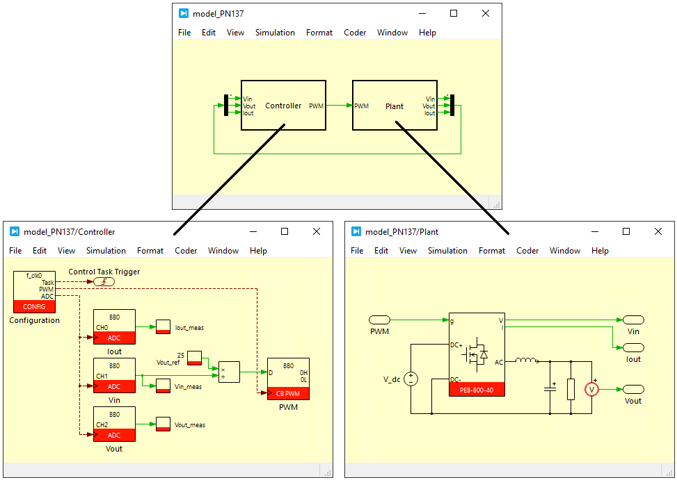
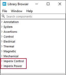
As explained in PN134, offline simulation is an optional but highly valuable step in control code development, enabling validation of control algorithms before deployment. This process relies on simulation models of both the Controller and the Plant that faithfully reproduce real-world behavior using specialized blocks from the Control and Power libraries included in the ACG SDK.
Imperix supports using the same PLECS model for both simulation and code generation purposes:
- In offline simulation, both the Control and Plant subsystems are simulated.
- In code generation mode (Build process), only the Control subsystem is compiled, and the Plant subsystem is ignored.
Fundamental concepts
To model the behavior of the overall system, the following fundamental concepts are used:
- Plant modeling (continuous domain): Plant quantities are generally modeled with continuous signals, as it is usually more efficient to simulate physical systems with wide-ranging dynamics. To support this, the model must be simulated using a variable-step solver.
- Control modeling (discrete domain): The control algorithms are modeled using discrete signals, sampled at the CPU interrupt frequency and shifted by the sampling phase.
- The Controller subsystem must therefore be configured as an Atomic subsystem, as this ensures its entire content executes as a single block at a common sample time (the interrupt period). The sample time configuration is explained later on this page.
- While this typically requires an algorithm implemented in the discrete-time ($ z$) domain, PLECS can automatically discretize continuous-time transfer functions. Consequently, both \(z\) and \(s\) domains can be used (and even coexist within the same controller subsystem). For instance, the following two models have strictly identical behaviors:
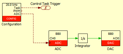
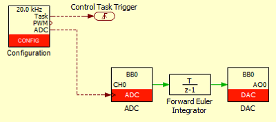
Control modeling
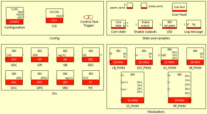
An accurate representation of the controller and its behavior is ensured by carefully modeling each of its peripherals. A fundamental part of the corresponding effort focuses on sampling and correctly accounting, in simulation, for the discrete execution of the control algorithms. Specifically, the following features are modeled:
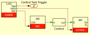
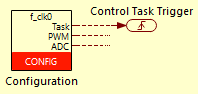
- Sampling (CONFIG and ADC blocks): Both the frequency and exact sampling phase are accounted for in simulation. This notably permits the accurate modeling of synchronous sampling. The sampling phase is imposed by the Control Task Trigger block, as detailed below.
- Algorithm execution (CONFIG block): The delay introduced by the computation of the control algorithms is modeled to ensure the overall controller delay is accurately captured. This value can be specified in the Cycle delay parameter of the CONFIG block.
- PWM generation (PWM block): The frequency, phase, and shape of the PWM carrier are accurately modeled, along with the update instants for duty-cycle and phase parameters. Optionally, dead time can also be simulated.
These three points directly follow from how imperix controllers physically operate, as detailed in PN261. More information about their firmware-level architecture is also given in PN253.
Plant modeling
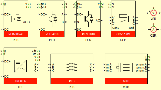
To test the developed control logic in offline simulation, a plant model is required. This model can be built using any PLECS circuit. To assist customers in deriving a model of their imperix power hardware, the Power library provides simulation models for all imperix power products. More information about that library is given in Getting started with the Imperix Power library.
Solver configuration
The variable-step solver used to run the offline simulation of both the Controller and Plant subsystems can be configured to manage time-step calculations and simulation accuracy. These parameters are accessible via the Simulation Parameters dialog (Ctrl+E).
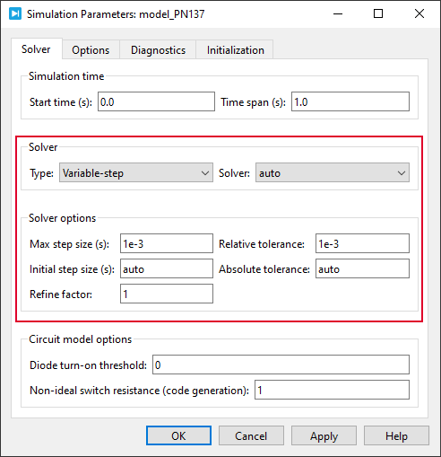
In most cases, the default settings are sufficient to simulate the model accurately. Specifically, the automatic solver selection (stiff vs. non-stiff) is typically the best choice, as it is efficient for non-stiff systems and automatically switches to a stiff solver if the system becomes stiff during simulation.
In most cases, the default values are sufficient. However, in some rare scenarios, manual adjustments may be necessary for the following reasons:
- Capturing fast transients: If rapid switching events are missed, lowering the Relative tolerance or the Max step size will force the solver to use higher precision and reduce the step size.
- Optimizing simulation speed: For long-duration simulations where high precision is less critical, increasing the Relative tolerance allows the solver to take larger steps, thereby reducing total simulation time. Obviously, this must be done carefully, since it may cause the solver to skip over critical high-frequency dynamics (e.g., PWM switching instants), resulting in significant inaccuracies in the simulated behavior.
Working principles of the main blocks
The four fundamental blocks are the 1) CONFIG, 2) Control Task Trigger, 3) ADC, and 4) PWM blocks. Most control implementations actually require only these four blocks, as in the base configuration shown below.
Configuration block (CONFIG)
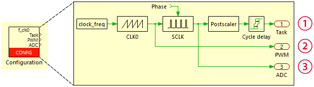
The CONFIG block defines the frequency and phase of the main clock source (\(F_{\text{CLK0}}\)) and manages sampling and CPU execution. This clock source can also serve as a reference for other peripherals, such as PWM modules, as explained further in PN259.
Specifically, the CONFIG block is used to configure the following parameters:
- Base clock frequency (\(F_{\text{CLK0}}\)): The primary timing reference for the system.
- Sampling phase (\(\phi_s\)): Shifts the sampling instant within the \(F_{\text{CLK0}}\) period.
- Interrupt postscaler (\(k_{\text{post}}\)): Optionally decimates the interrupt execution frequency.
- Cycle delay: Represents the specific computation time required by the control algorithm.
The resulting hardware-level operational parameters are defined as:
- Sampling clock: Operates at frequency \(F_{\text{SCLK}} = F_{\text{CLK0}}\) with a sampling phase of \(\phi_s\).
- CPU interrupt: Triggered at frequency \(F_{\text{CPU}} = F_{\text{CLK0}}/k_{\text{post}}\) with a phase of \(\phi_s\).
In PLECS' simulation environment, these hardware parameters are carried using brown wires, which are used for the following configuration signals:
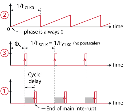
- Base clock CLK0 (label ②): Modeled using a sawtooth generator. This signal is output via the PWM port and wired to the PWM modulators.
- Sampling clock (label ③): Generated from CLK0, shifted by the sampling phase parameter. This output is intended to be connected to ADC blocks to specify the exact sampling instants.
- Control task trigger signal (label ①): Generated from the sampling clock and delayed by the Cycle delay parameter. This signal represents the "end of interrupt" and must be connected to the Control Task Trigger. Including the Cycle delay enables the simulation to accurately model latency due to interrupt execution time and various read/write delays, as explained in the following section.
Cycle delay
The Cycle delay specified in the CONFIG block dialog is a parameter used only for simulation. It is introduced to simulate the delay from the moment the ADCs are sampled to the moment the calculated duty-cycles are propagated to the FPGA PWM management. It takes into account the ADC sampling time (e.g. 2 µs on a B-Box RCP), the control algorithm execution time, and the FPGA read and write transfer time.
The total cycle delay is displayed in the Timings tab of Cockpit when a code is running.
Control Task Trigger and interrupt frequency
The Control Task Trigger is a mandatory block that must be connected to the Task output of the CONFIG block. It defines when the control task starts, thereby ensuring that the sampling and interrupt phases are modeled correctly.
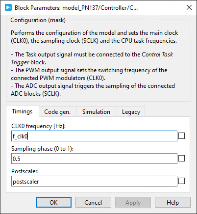
The discretization period, corresponding to the CPU's execution rate, is defined in the Scheduling tab of the Coder Options dialog. For correct execution, this parameter must match the parameters defined in the CONFIG block, as there is no automatic transfer of configuration parameters between them.
To ensure the configuration remains consistent, use the model variables defined in the Initialization tab of the Simulation Parameters dialog, as shown below. This approach is used in the template file provided at: C:\imperix\BB3_ACG_SDK\plecs\imperix_template.plecs.
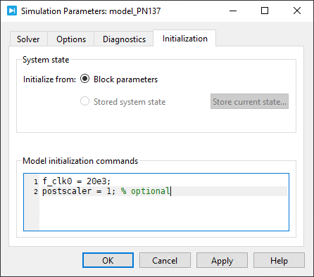
These variables are referenced in both the CONFIG block and the Coder Options dialog, as illustrated below.
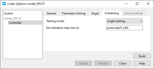
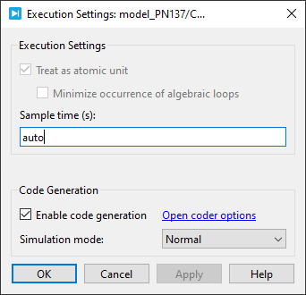
Finally, setting the Sample time of the Controller atomic subsystem to auto ensures that the subsystem runs at the rate specified in the Coder Options dialog.
Analog-to-digital converter input (ADC)
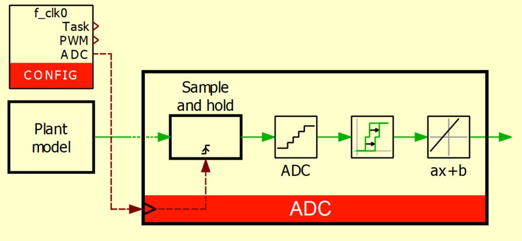
At the hardware level, each ADC block accesses a continuous variable representing a physical measurement, samples it at the desired sampling instant, and feeds it to the CPU for processing. The variable then becomes a discretely sampled value.
To accurately model this in simulation, the ADC block sample-and-holds the input signal at the rising edge of the ADC trigger input, and produces a discrete signal at its output. If Simulate sensor(s) sensitivity(ies) is enabled, the sampled signal is also scaled according to the sensor sensitivity parameter to obtain its value in physical units (e.g. Volts or Amperes).
Regarding the scaling of measurements, two approaches are possible:
- Sensor sensitivity is not modeled: the sensor in the Plant outputs the measurement in its physical unit (e.g., V or A). In this case, the ADC block does not need to apply any scaling to retrieve the measured value, and the Simulate sensor(s) sensitivity(ies) option should be disabled. This approach is simpler and is useful for algorithm development or early-stage testing.
- Sensor sensitivity is modeled as follows: the sensor in the Plant outputs the measurement scaled by its sensitivity. In this case, the ADC block must apply the same scaling to retrieve the measured value, and the Simulate sensor(s) sensitivity(ies) option should be enabled. This approach is useful, for example, to validate that measurements remain within the controller's analog input range, and is particularly important for offline validation in HIL testing to ensure that the analog signal scaling is correct.
Pulse-width modulators (xx-PWM)
Various types of pulse-width modulators are available in the Imperix control library. Among them, the carrier-based PWM (CB-PWM) block is the most commonly used.
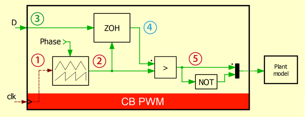
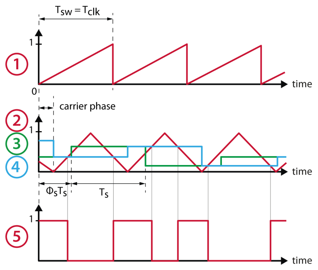
In the simulation model, the clock signal ① serves as the frequency and phase reference to generate the carrier signal ②. In parallel, the duty-cycle value ③ is sampled once or twice per switching period (depending on the update-rate parameter, see PN259), yielding the signal ④, which is subsequently compared with the carrier to produce the output PWM signal ⑤. If Simulate dead time is selected in the Dead time simulation mask parameter, a dead time is inserted between the complementary signals.
Further readings
The following related articles are recommended:
 By Julien Orsinger • December 15, 2025 • PN134