Table of Contents
This quick-start guide describes how to build a buck converter controlled in open-loop using power modules and the B-Box RCP 3.0 programmable controller using the Simulink blockset. Specifically made for users who would want to get familiar with imperix’s solutions, this guide details step-by-step instructions on how to assemble and program a simple power converter. Further details on the theoretical aspects of buck converters can be found on the page: Step-down buck converter. An HIL implementation of a buck converter is provided in TN178.
Hardware requirements
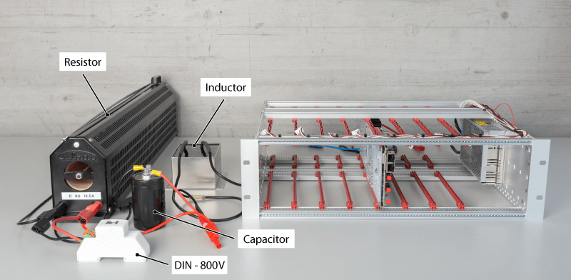
The following list describes the required hardware to build a buck converter. It comprises imperix products as well as additional components commonly available in power electronic research laboratories :
- Imperix products
- 1x programmable controller (B-Box 4 or B-Box RCP 3.0 or B-Box Micro)
- 1x phase-leg module (PEB-800-40 or PEB8038 or PEB8024 or PEB4050)
- 1x voltage sensor (DIN-800V or VSR-1000)
- Control development tools for Simulink and PLECS (ACG SDK), with a valid license
- Additional hardware
- 1x Inductor
- 1x Capacitor
- 1x Resistor
- A power supply
- Safety laboratory cables (banana)
(Power supply and passive components not sold by imperix)
Description of the implemented system
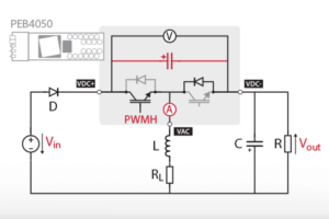
The schematic below serves as a reference for the required electrical connections. It is a buck converter made from a semiconductor switching cell, an inductor, a capacitor, and a load resistor. The converter is operated in open-loop by a programmable controller, a B-Box RCP 3.0 in this specific case.
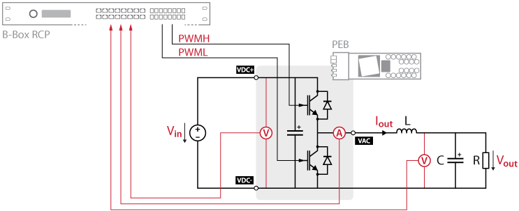
As opposed to a buck made with a diode and a transistor, this one is made with a commutation cell (two transistors). In other words, the bottom transistor’s body diode acts as a freewheeling diode, to reduce the voltage spike across the inductor.
Note that, in the case of MOSFETs, their body diodes are known to perform poorly and will generate significant losses when the upper switch is open. To avoid this issue, a PWM signal also drives the low-side transistor so that the current goes through the channel and not the body diode.
In this case, the operating conditions for the converter were defined by the load resistor current rating of 13.5 [A]. Having a resistance of 8.5 [Ω] and a low-voltage (\(V_{out}\)) of 100 [V], a maximum load current of 11.75 [A] is achieved. An off-the-shelf inductor and capacitor of 2.36 [mH] and 2 [mF] respectively, guaranteed Continuous Conduction Mode (CMM) operation and acceptable output voltage ripples.
Mechanical assembly of the power equipment
The first step to build the converter is to connect a cable to the VAC terminal (switching midpoint) of the PEB module. It is best to do it before inserting the module into the mounting rack, as the switching midpoint will be hard to reach then. A safety banana cable terminated by a ring terminal could be used as cable, which will be screwed with a small M4 screw to secure the wire. This allows an easier connection with other equipment. Two similar cables can be connected in the same way to the VDC+ and VDC- power terminals and the power supply.
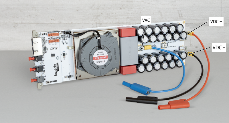
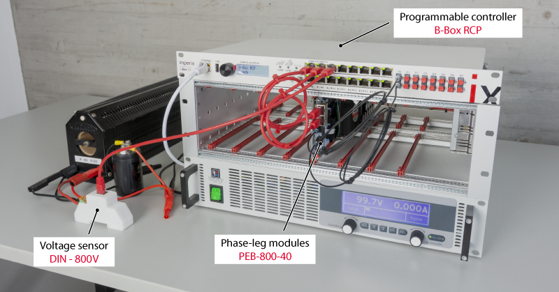
Next, the user can insert the power module into the mounting rack as shown below. The auxiliary power supply cable from the rack also has to be connected to the module.
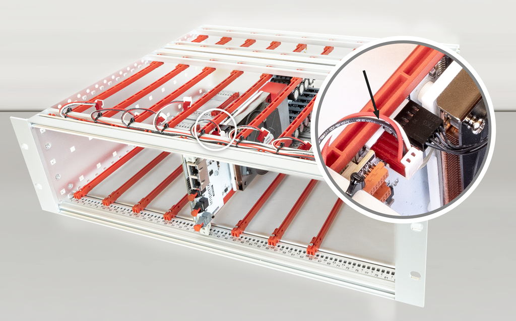
Note that, in this specific case, only one module is required. But for applications with several modules, a grey flat wire connects the modules for fault propagation, as shown in the picture below. More information about how to expand an open rack can be found here.
Flat cable connection for fault propagation between modules
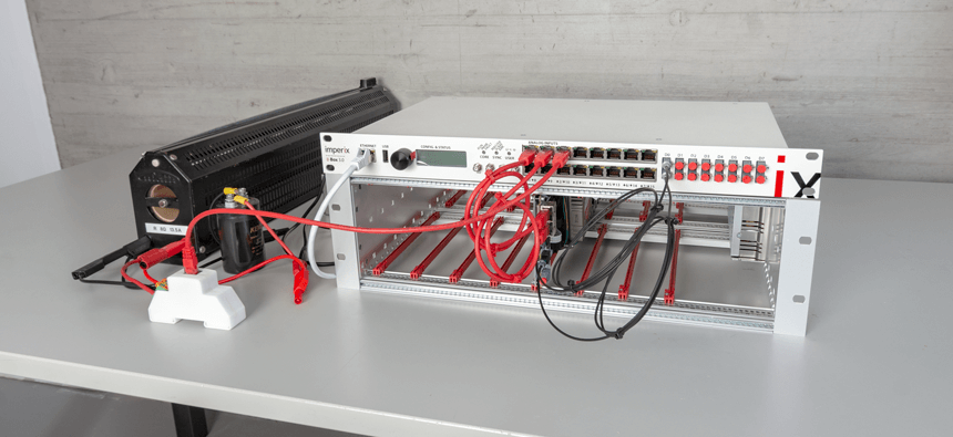
The next step is to wire the components according to the converter’s schematic. The following picture shows a connection example.
Connection to the controller
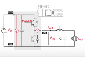
The rapid prototyping controller (B-Box RCP) connects to the power module as described in the table below.
| Signal | Type | Controller side | Converter side |
|---|---|---|---|
| \(PWMH\) | PWM | Optical output D0H | Gate H optical receiver |
| \(PWML\) | PWM | Optical output D0L | Gate L optical receiver |
| \(I_{out}\) | Measurement | Analog input 0 | PEB RJ45 port (top) |
| \(V_{in}\) | Measurement | Analog input 1 | PEB RJ45 port (bottom) |
| \(V_{out}\) | Measurement | Analog input 2 | DIN-800V RJ45 port |
The following picture shows the connections once completed.
Finally, the control algorithm is uploaded to the B-Box RCP 3.0 via its Ethernet port, connected to the computer either directly or through a local network. Further details regarding the connection of imperix controllers to the host computer can be found in PN138.
Configuration of the analog inputs
Before doing any experiments, it is essential to properly configure the analog input channels of the B-Box RCP 3.0. These channels have both hardware and software settings. The hardware settings can be configured from the B-Box RCP 3.0 front panel, and the software settings are configured inside the Simulink or PLECS control model.
Software settings
- Channel number
- Sensor type
- Programmable gain
- Sensitivity and offset
- Sampling strategy
Hardware settings
- Input impedance
- Low-pass filter activation
- Gain (must match the software setting)
- Safety limits (upper and lower thresholds)
More information about the ADC block of Simulink and PLECS blocksets can be found here. Additionally, related information on the analog I/O configuration on B-Box 4 can be found in PN105.
The configuration of the three analog input channels for this application is summed up in the table below.
| Measured signal | Input channel number | Low impedance | Gain | Filter | Limit high [V] | Limit low [V] | Disable safety | Save |
|---|---|---|---|---|---|---|---|---|
| \(I_{out}\) | 0 | no | x4 | no | 2.4 | -0.2 | no | yes |
| \(V_{in}\) | 1 | no | x4 | no | 2.5 | -0.1 | no | yes |
| \(V_{out}\) | 2 | no | x4 | no | 1.2 | -0.1 | no | yes |
Development of the control software
Installation and setup of the computer software
Two pieces of software are required: the imperix Automated Code Generation Software Development Kit (ACG SDK), which can be downloaded here, and a compatible version of Matlab (2016 and newer), including the following toolboxes:
- Matlab Simulink
- Embedded coder
- Matlab coder
- Simulink coder
A detailed guide on how to set up the software is provided in the Installation guide for imperix ACG SDK.
Simulink model configuration
The control model, shown below, implements a simple open-loop operation of the buck converter. Since the converter is designed in continuous conduction mode, the step-down ratio corresponds to the duty cycle:
$$d = \frac{V_{out}}{V_{in}} $$
The duty cycle for the PWM can therefore be calculated by dividing the reference output voltage by the measured input voltage. This allows the user to set a desired output-voltage reference while the controller automatically computes the corresponding duty cycle. Details on closed-loop control are provided in TN105.
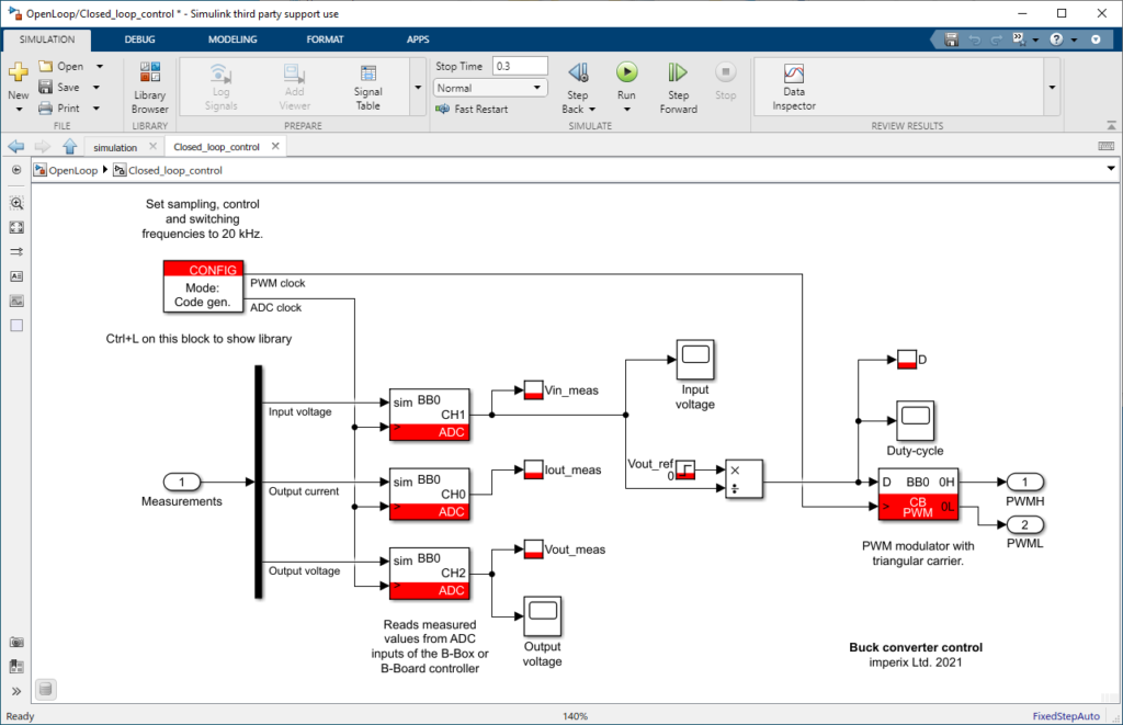
The following sections provide information on the necessary blocks needed to build such a control algorithm for a buck converter. The user can program the controllers using Simulink or PLECS, as aforementioned. This guide will focus on Simulink, but both programming options are introduced here.
User template
To start working with Simulink, one can find a project template in: “C:\imperix\BB3_ACG_SDK\simulink\user_template\imperix_template.slx”
This template is preconfigured for code generation for imperix controllers. It should then be copied into the desired working directory and renamed. When opening this file, a controller and a plant block are displayed as shown below.

The plant block contains the simulation model of the circuit and will not be detailed here. Further information can be found in Simulation essentials with Simulink (PN135). The controller block is the one of interest since it is the model of the actual real-time code.
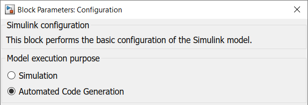
The CONFIG block
The CONFIG block, already present inside the controller block, performs the basic configurations of the model. It is by default set to simulation. This parameter needs to be changed to code generation to program the B-Box RCP 3.0.
The ADC block
The ADC block is used to retrieve the measurements from the analog inputs of an imperix controller. In this case, three ADC blocks are used, one for each measurement, and have been configured as follows:
| ADC 0 | |
|---|---|
| Device number | 0 |
| Input channel | 0 |
| Sensor | Current PEB 8038 |
| Gain | x4 |
| ADC 2 | |
|---|---|
| Device number | 0 |
| Input channel | 2 |
| Sensor | Voltage DIN-800V |
| Gain | x4 |
| ADC 1 | |
|---|---|
| Device number | 0 |
| Input channel | 1 |
| Sensor | Voltage PEB 8038 |
| Gain | x4 |
The PWM block
The PWM signals are generated by the carrier-based PWM block (CB PWM) and drive the power transistors. In this case, the PWM outputs are set to channel 0. Moreover, since both of the module’s transistors are switched, the output mode is set to Dual. The carrier type is set to triangle, and the update rate is set to single (one update instant happening at the zero of the carrier).
The tunable parameter and probe blocks
The last two blocks used are the tunable parameter and the probe block. The tunable parameter is used to let the user set the voltage reference in real-time, while the code is running. The probe is used to monitor the desired signal, in real-time as well, in Cockpit.
Generation and real-time execution of the controller code
Once the simulation has been validated, the user can generate the code to be uploaded to the controller by pressing Ctrl + B on Simulink (Ctrl + Alt + B on PLECS). This will automatically generate the C code that is then compiled, loaded, and launched on the selected target. It also launches Cockpit, imperix’s monitoring software. More information on the latter can be found in the corresponding user guide.
The user will then need to link the new project to the controller (target). After this, the code will automatically start. At this point, users can drag variables from the sidebar list into visualization modules, such as the Scope or Rolling Plot, allowing them to monitor signals and operate the converter in real time.
A first test could be performed to check that the hardware protection limits are correctly configured on the analog frontend of the B-Box RCP 3.0. This test consists of lowering the protection limits on the analog front end to more conservative values and verifying that the PWM signals are indeed disabled when these limits are exceeded.
Subsequently, one can turn on the power supply and slowly increase the voltage to 100 [V]. To make sure that the input voltage measurement is correct, the user could verify that \(V_{in}\) is indeed close to 100 [V] on Cockpit. The last step is then to set a value for the reference voltage, 25 [V] for instance, and press the enable PWM switch on the upper left corner of Cockpit. A measured output voltage of around 25 [V] should be visualised. Due to the diode voltage drop and other non-idealities, this value will not reach the theoretical value.
Experimental results
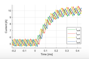
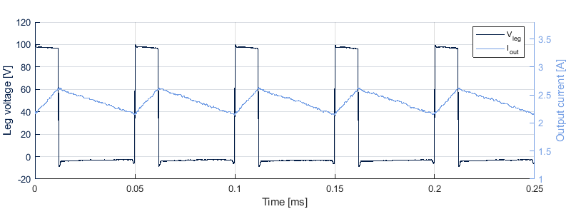
The plot below shows the leg voltage as well as the output current of the buck converter built above. With a duty cycle value of 0.25, it is clear on this graph that the input voltage of 100[V] is applied to the output only during a fourth of the control period. This results in an output voltage of 25[V].
To go further…
The next possible step could be to add two power modules to build a three-phase voltage source inverter (VSI) like the one in TN152. A guide, similar to this one, on the assembly of a three-phase inverter is available here: How to build a 3 phase inverter. One could then combine the VSI with a boost converter to create a Three-phase PV inverter for grid-tied applications (AN006), which showcases the great potential of imperix’s solution for modular power converters. Finally, the interleaving of several buck converters and the implementation of proper current control techniques are discussed in Interleaved buck converter current control.