Table of Contents
This application note details a control implementation for a back-to-back three-phase converter developed using imperix’s rapid control prototyping solutions. The system features two TPI8032 (TPI) converters managed by a single centralized controller in a master/slave configuration.
In this implementation, the grid-side converter operates as an active front end and is connected to the grid in a transformer-less fashion via an LCL filter. On the other side, the load-side converter functions as an inverter that drives a simple RL load.
System principles and control architecture
This section describes the back-to-back converter topology and the centralized control architecture used to manage the system. The simplified diagram of the back-to-back converter is shown in Fig. 1. Such converters are commonly employed in wind energy systems, HVDC links, and industrial variable frequency drives to enable bidirectional power transfer and regenerative operation.

Back-to-back converter Topology
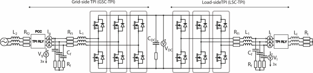
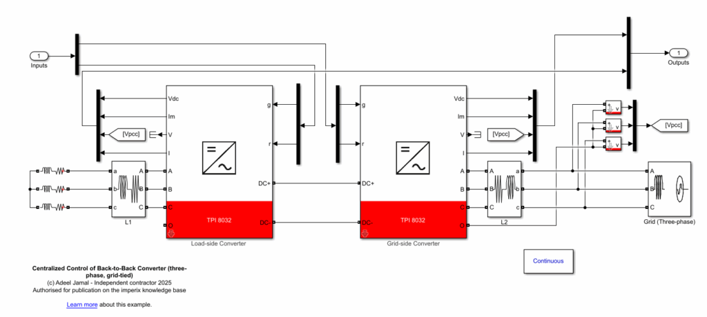
A back-to-back converter consists of two three-phase converters, typically an AC/DC rectifier stage and a DC/AC inverter stage, connected via a common DC link. The detailed three-phase diagram of the system is illustrated in Fig. 2. This configuration effectively decouples two AC systems, allowing for independent control of power flow, frequency, and voltage. In this application, both converters are implemented using the imperix TPI8032 three-phase power converter; therefore, the DC link capacitors of both are connected in parallel, resulting in a doubling of the DC link capacitance.
The DC link is shared between the two TPIs, as shown in Fig. 2. The system is composed of the following:
Grid-side converter (GSC):
GSC operates as an active front end. It is connected to the three-phase grid through an LCL filter. Since TPI already has an equivalent LC filter, the output of TPI is connected to the grid via an external choke of \(L_2\) = 0.65mH, as shown in Fig. 2. This configuration is similar to the one described in TN123. The primary role of GSC is to regulate the DC link voltage while ensuring high-quality current absorption from the grid (i.e., low harmonic distortion and unity power factor), which is enabled by the LCL filter.
Load-side converter (LSC):
LSC draws power from the DC link to supply a passive three-phase load. It is controlled to provide a preset value of AC current to the load. In this application note, RL is used as a load. This allows the application example to be generic. Typically, this second converter may also be part of a drive (see, for instance, AN004, which addresses the direct torque control of a permanent magnet synchronous machine).
Centralized control architecture
The system employs a centralized control architecture for the back-to-back converter, where the entire control algorithm is implemented on a single master controller. The core of this system is a TPI8032 programmable converter, which contains a B-Board PRO embedded converter controller for executing the control code. While two TPI8032 converters are used, they operate in a master-slave configuration, also called I/O extension mode:
- One TPI8032 acts as the master, with its CPU running the complete control algorithm for the entire back-to-back converter system. TPI8032 controller samples all necessary measurements, including grid voltages, grid currents, DC link voltage, and load currents. It executes the control algorithms for both the GSC and the LSC within the same control cycle and then generates and sends PWM signals to both TPIs simultaneously.
- The second TPI8032 functions as a slave unit. In this mode, the TPI controller operates as a simple I/O extension, with only its FPGA active to manage inputs and outputs as directed by the master. The slave unit does not run its own control code.
The communication between two TPIs leverages imperix’s RealSync communication protocol, which uses an SFP optical fiber link to ensure low-latency, deterministic data exchange and precise synchronization between the two devices. This centralized approach is distinct from a coordinated control strategy (see multi-master). Refer to technical note TN155 for more details on implementing coordinated control of a back-to-back converter with two separate controllers.
Control implementation
The chosen control scheme here is divided into two parts: one for the GSC and another for the LSC, described as follows:
Grid-side converter control
The control for the GSC uses a cascaded structure to achieve voltage regulation of the DC bus, similar to active front end control. Refer to TN108 for further details about the cascaded control strategy.
DC bus voltage control
The outer control loop consists of a PI controller and a feedforward of the load current to maintain the DC link voltage at its reference value, as shown in Fig. 3. The implementation of feedforward of the load current in the DC link voltage controller becomes possible thanks to the centralized controller architecture. The deviation in the controlled DC link voltage is drastically reduced by feedforwarding the load current from the LSC.
Grid current control
The inner loop, based on proportional resonant control in parallel to the active damper, regulates the grid current to follow the reference generated by the outer voltage loop. The reactive current reference is typically set to zero to ensure unity power factor operation. The principles of the cascaded control loop design are further detailed in TN108.

An active damping strategy is implemented to mitigate the natural resonance of the LCL filter, which can otherwise cause instability and current oscillations. The design described in the technical note TN123 is replicated to achieve damping by feeding back the grid current.
Load-side converter control
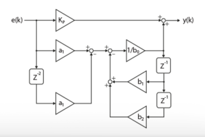
In this application note, LSC is responsible for delivering a precisely controlled three-phase AC current to the passive R load. This is achieved using a vector current control strategy implemented in the synchronous rotating (dq) reference frame. The block diagram of the load current control is shown in Fig. 4. The three-phase load currents are measured and transformed into DC quantities using the Park transformation.

Two separate PI controllers are used to regulate these DC quantities in their respective reference frames. This approach is effective because PI controllers can regulate DC values with zero steady-state error. The outputs of the PI controllers are then transformed back into the abc reference frame for the TPI CB-PWM modulator.
DC link precharging
As with any voltage source converter topology, the system requires that the DC bus be appropriately pre-charged before normal operation can be initiated (\(V_{DC,min}=\widehat{V_{g,ll}}\)). The TPI relay block is used to pre-charge the DC link with safety protections already embedded inside the TPI, with a set of three resistors that limit the DC bus charging current. These resistors are bypassed during normal operation, thanks to a state machine of the TPI relay. TN131 provides additional recommendations for system start-up techniques in grid-tied applications if imperix power modules are to be employed.
Software resources
The control of the back-to-back converter is implemented in MATLAB Simulink using the imperix ACG SDK.
AN005_B2B_converter_centralized_control_Simulink.zip file contains the complete MATLAB Simulink model for the entire back-to-back converter system, including all files required for both simulation and automated code generation. The GUI file to be used in the imperix Cockpit is also provided.
Simulation results
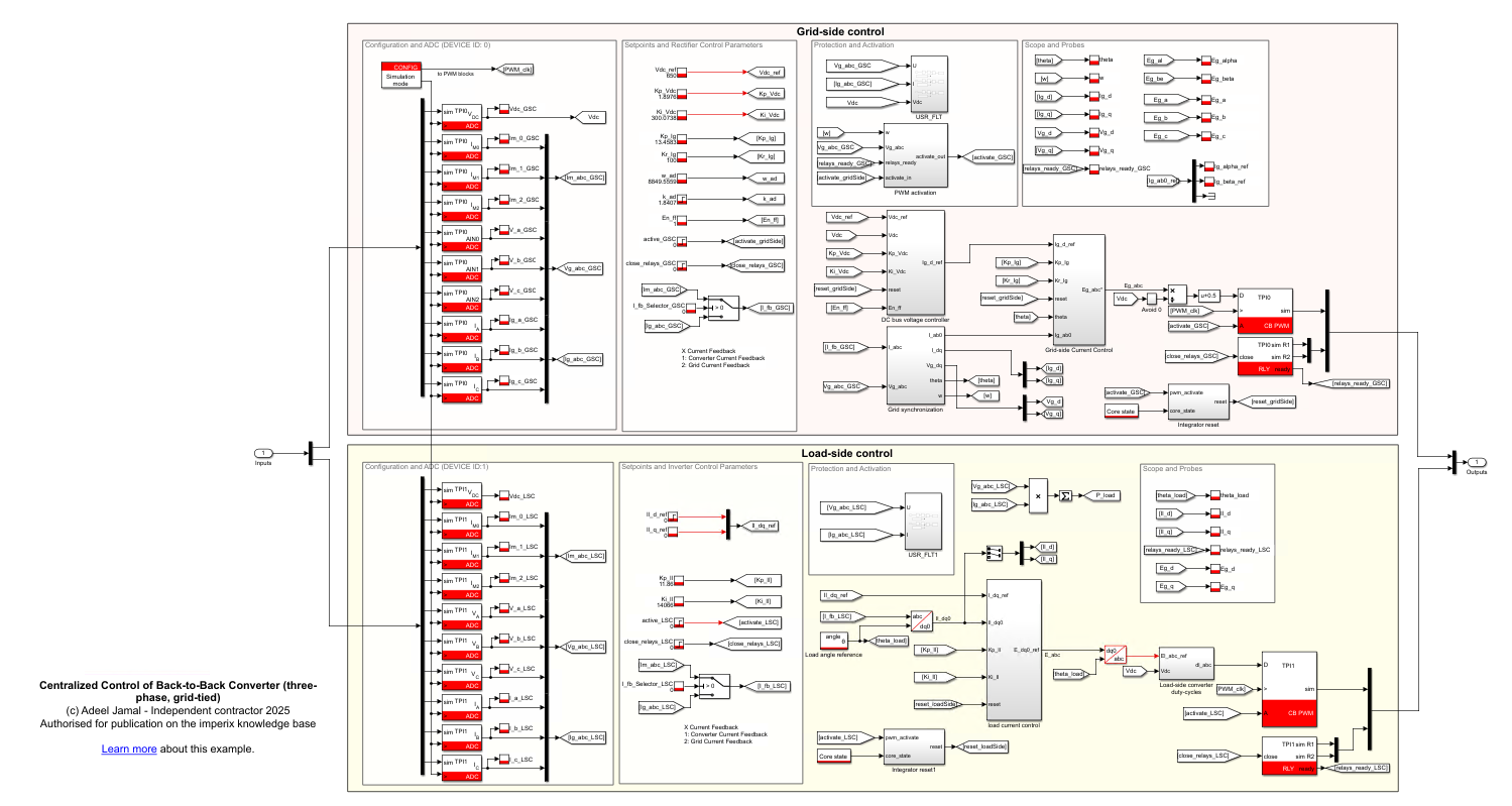
The performance of the back-to-back converter control is simulated using Simulink. Two separate controllers, one for the GSC and the other for the LSC, are designed, as indicated by the differently colored area containers shown in Fig. 5. Two TPI blocks available in imperix’s power library are used to build the model of the back-to-back converter on the plant side, as depicted in Fig. 6. The system and control parameters are summarized in Table 1.
| Parameters | Value | Parameters | Value |
|---|---|---|---|
| Grid voltage (line-to-line) | 400 VRMS | Grid frequency | 50Hz |
| Inverter side inductor L1 | 1.05mH | Grid side inductor L2 | 0.65mH |
| Capacitor Cf | 8.2µF | L2 coil resistance Rf2 | 100mΩ |
| Grid inductor Lg | 10µH | L1 coil resistance Rf1 | 54mΩ |
| Equivalent capacitor resistance (Rf) | 10Ω | DC link capacitor (CDC ) | 2 x 1.5 mF |
| Control/switching frequency \(f_s\) | 50kHz | DC bus voltage VDC | 650V |
| Proportional gain-grid current (PR controller) kp,ig | 5V/A | Resonant gain-grid current (PR controller) kr,ig | 100Vs/A |
| Active damping gain kAD | 1.84 | Active damping pulsation ωAD | 18850 rad/s |
| Load resistor RL | 27Ω | Load Inductor Ll | 1 mH |
| Integral gain-DC voltage controller ki,dc | 300 | Proportional gain-DC voltage controller kp,dc | 1.89A/V |
| Integral gain-load current controller ki,il | 14066 | Proportional gain-load current controller kp,il | 11.86 V/A |
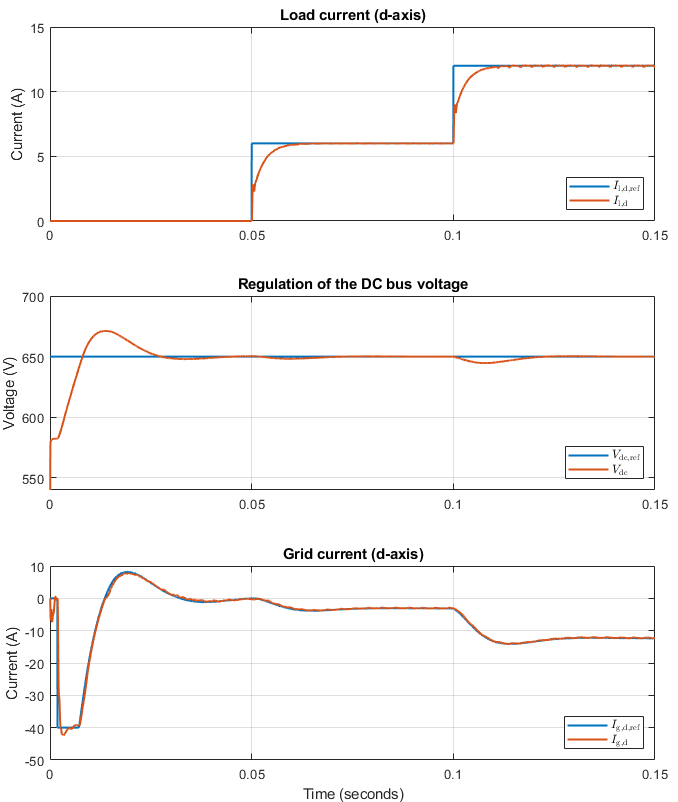
A reference load current step in d-axis from 0A to 6A is applied at t = 50 ms, and a step from 6A to 12A at t = 100 ms. During the transient, a voltage drop of 1.5V-2V can be observed on the DC bus voltage. The DC link voltage control corrects this voltage drop. In this application example, the current drawn by the load-side inverter is feed-forwarded into the DC link voltage control. The introduction of such compensation improves the control dynamics and reduces the deviation in the voltage drop.
Analyzing the simulation results shown in Fig. 7, the grid currents (d-axis) follow their references with a minimal instantaneous error. The grid current is measured as positive, flowing from the DC link to the grid. During the transient, as well as during steady-state, the q-component of the grid current is zero, as specified by the reference (Ig_q_ref = 0). The load current Il_d reaches its reference in around 10 ms (100% of the final value), following the same behavior as a step response of a first-order system.
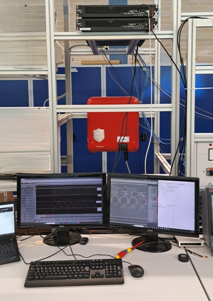
Experimental Setup
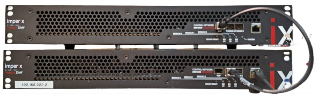
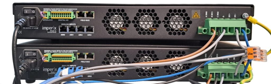
The TPI8032 is connected via an external choke L2 to the grid. GSC is used to power up the DC link. Three external voltage sensors are placed at the PCC to measure the grid voltage. The following list describes the required hardware and software. It comprises imperix products as well as additional components commonly available in power electronic research laboratories:
- Imperix products
- 2x TPI8032 (Three-phase fully programmable inverter)
- Control development tools for Simulink (ACG SDK)
- Minimum requirements: Imperix ACG SDK 2025.1 or newer.
- Cockpit to monitor and debug
- Additional software
- Matlab Simulink with relevant toolboxes.
- Minimum requirements: MATLAB Simulink R2019a or newer.
- Matlab Simulink with relevant toolboxes.
- Additional hardware
- 3x grid inductor/chokes (L2 = 0.650 mH)
- 3x DIN voltage sensors
- Safety laboratory cables (banana)
- 1x SFP cable
- 3x load resistors (Rl = 27Ω)
- 3x load inductors (Ll = 1 mH)
Note that if the grid inductor value is different, the controller and active damper gain have to be tuned accordingly; refer to TN123 for further details. For more information on how to get started with TPI8032, please refer: PN190: Getting started with the TPI 8032. The DOWN of GSC-TPI should be connected to the UP of LSC-TPI ideally, as shown in Fig. 8(a). It can be noticed in Fig. 8(b) that the external DIN voltage sensors are connected to the three analog inputs of the GSC-TPI: AIN0, AIN1, and AIN2 for measuring the voltage at PCC.
Experimental results
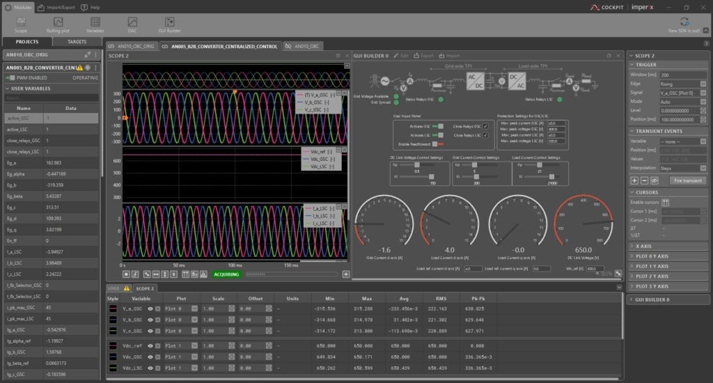
The experimental validation of the back-to-back converter system was performed using the setup shown in Fig. 9. The Cockpit GUI designed for ease of operation is shown in Fig. 10. The system can be started using the defined start-up procedure explained in the operating instructions section.
The TPI Relays of both converters were closed after the DC link was pre-charged and the PLL synchronized with the grid voltage. The DC link voltage is then stabilized around its reference value of approximately \(650~\text{V}\) as shown in the second subplot of Fig. 11. Feedforward is enabled for this experiment. The deviation of the DC Link is less than 2V when the load current changes, thanks to the feedforward compensation of the load current. The phase voltages at the PCC, illustrated in the first subplot, are balanced and sinusoidal with a \(120^{\circ}\) phase displacement.
As in the simulation, there is zero reactive power exchange with the grid, as defined by its zero quadrature reference value \(I_{g,q,ref}=0\). Other reference setpoints can be specified to adjust the power factor or reactive power as required.
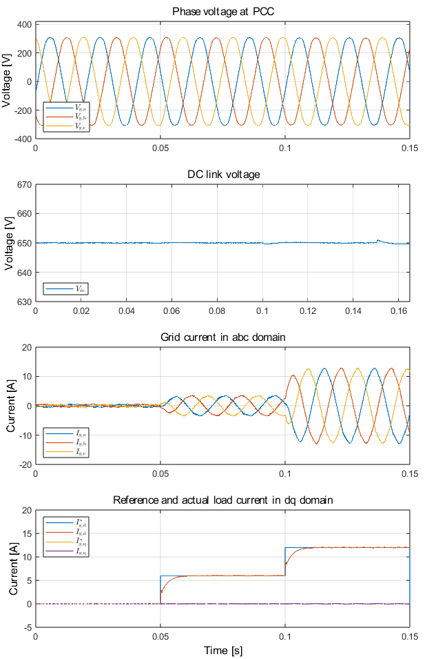
After verifying the DC-link voltage regulation, the load-side converter (LSC) was activated to control the load current in the dq domain. The bottom subplot shows that load currents (\(I_{l,d}\), \(I_{l,q}\)), closely follow their respective reference values. The grid currents in the abc domain (third subplot) remain sinusoidal and balanced once the LSC begins drawing power, confirming stable power transfer through the DC link.
The load current ripple is normally larger than the grid current ripple if the switching frequency is low, such as 10 kHz. Overall, the experimental results verify the correct operation of the cascaded control architecture, comprising the outer DC-link voltage controller and inner current control loops.
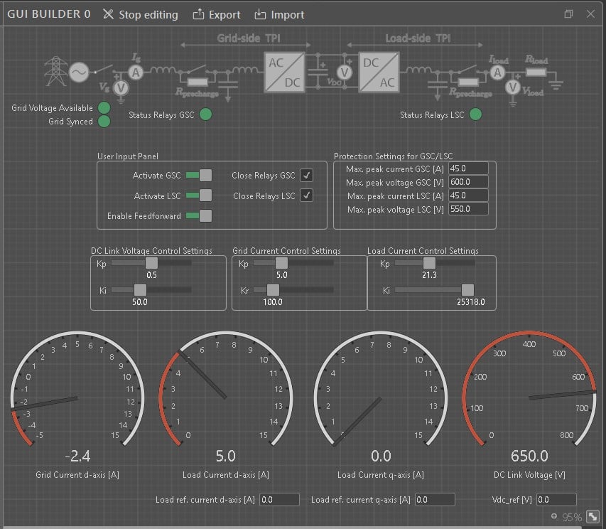
Operation and design of the GUI
The GUI shown in Fig. 12 provides the following features and functionalities:
- Operational controls for the GSC and LSC: activation toggles, relay close checkboxes, PWM enable, and feed-forward option.
- Protection settings for each TPI (GSC / LSC): numeric fields for maximum peak current and voltage limits. Default example values are provided in the GUI (GSC: Ipk 45 A, Vpk 600 V; LSC: Ipk 45 A, Vpk 550 V).
- Controller tuning panel with sliders and numeric entries for PI gains (DC-link, grid current, load current).
- Setpoint inputs beneath gauges for DC-link voltage (vdc_ref) and load current references (Il_d_ref, Il_q_ref).
- Status indicators: the top panel shows a system schematic with LEDs indicating Grid Available, Grid Synced, Status Relays GSC, and Status Relays LSC.
- Grid Voltage Available — grid present.
- Grid Synced — PLL locked and phase order correct.
- Status Relays GSC / LSC — relay closed and pre-charge complete.
- Real-time visualisation: circular gauges for peak d/q currents (grid & load) and a large DC-link voltage gauge for quick status.
GUI design can be modified according to the user’s requirements. Please refer to PN304 for more information on how to build or modify the GUI. More information on how to develop a GUI using Matlab App Designer is given in PN130.
To go further from here…
For learning more about the coordinated control of a back-to-back converter, refer to TN155. If you are interested in multi-master-based control, please check AN008.
TPI8032 can also be used to program any controller for grid-connected converters. More examples of the TPI8032 are available in the knowledge base for various applications, such as:
TN123: Active damping of LCL filters
TN163: Active power filters for harmonics mitigation