
Table of Contents
This page presents the firmware architecture of imperix controllers and details their corresponding data paths. Indirectly, this provides useful insights into how these devices operate, complementing the information in PN261, which addresses their operating principles.
System architecture
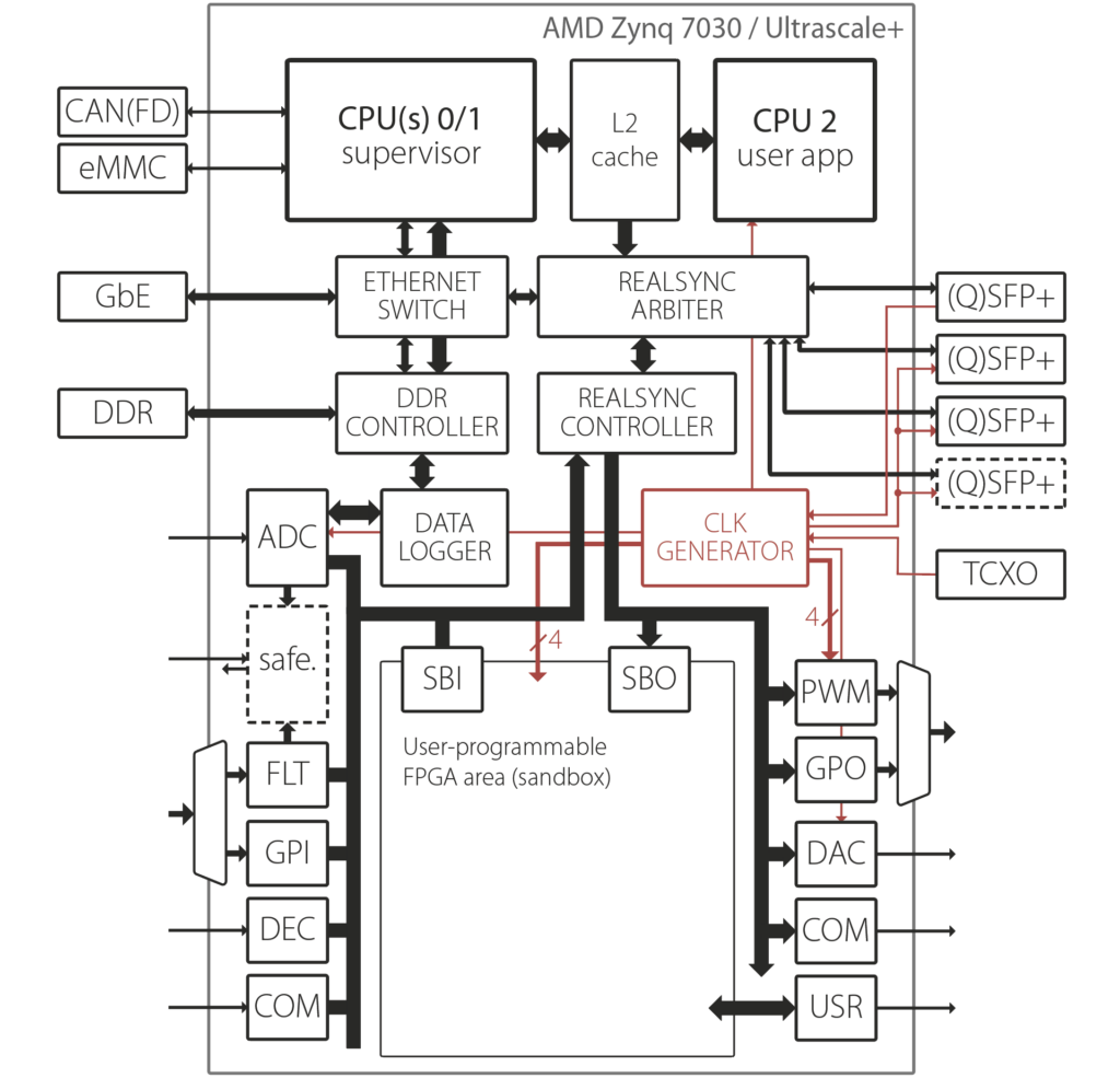
All imperix controllers are based on AMD Systems on Chip (SoC), which combine a high-performance Processing System (PS) with generic Programmable Logic (PL) on the same die:
- The processing system (PS) leverages fast CPU cores to perform floating-point arithmetic operations quickly. Since imperix controllers are multi-core systems, one core is fully dedicated to running user-defined control algorithms, and the other cores are responsible for system monitoring and data logging. Specifically, the task distribution is as follows:
- User application CPU: runs the control algorithms in a bare-metal, interrupt-based, hard real-time environment. It can be programmed by the user using Simulink, PLECS, or C/C++.
- Supervisor CPU(s): handle housekeeping tasks such as data logging, system monitoring, and starting/stopping user code. It also supports communication protocols such as Ethernet, CAN, and Modbus. The supervisor is mostly piloted by Cockpit. It cannot be programmed by the user.
- The programmable logic (PL) area is used to implement specialized functions at the hardware level, with absolute determinism and a very high temporal resolution. This notably concerns pulse-width modulators (PWM), I/O peripheral drivers, etc. By offloading as many tasks as possible to the PL, the available CPU time (and hence the achievable performance) is maximized. The PL is further partitioned into two areas:
- Pre-implemented logic: contains the non-editable hardware peripherals required for the proper operation of the controller.
- User-editable logic (sandbox): represents a dedicated programmable area where users can implement custom FPGA logic for advanced applications.
Although the selected SoC isn’t the same across all imperix controllers, their architectures are very similar, as shown below. The main differences lie around the analog acquisition stage, which has been significantly improved with the introduction of the B-Box 4.
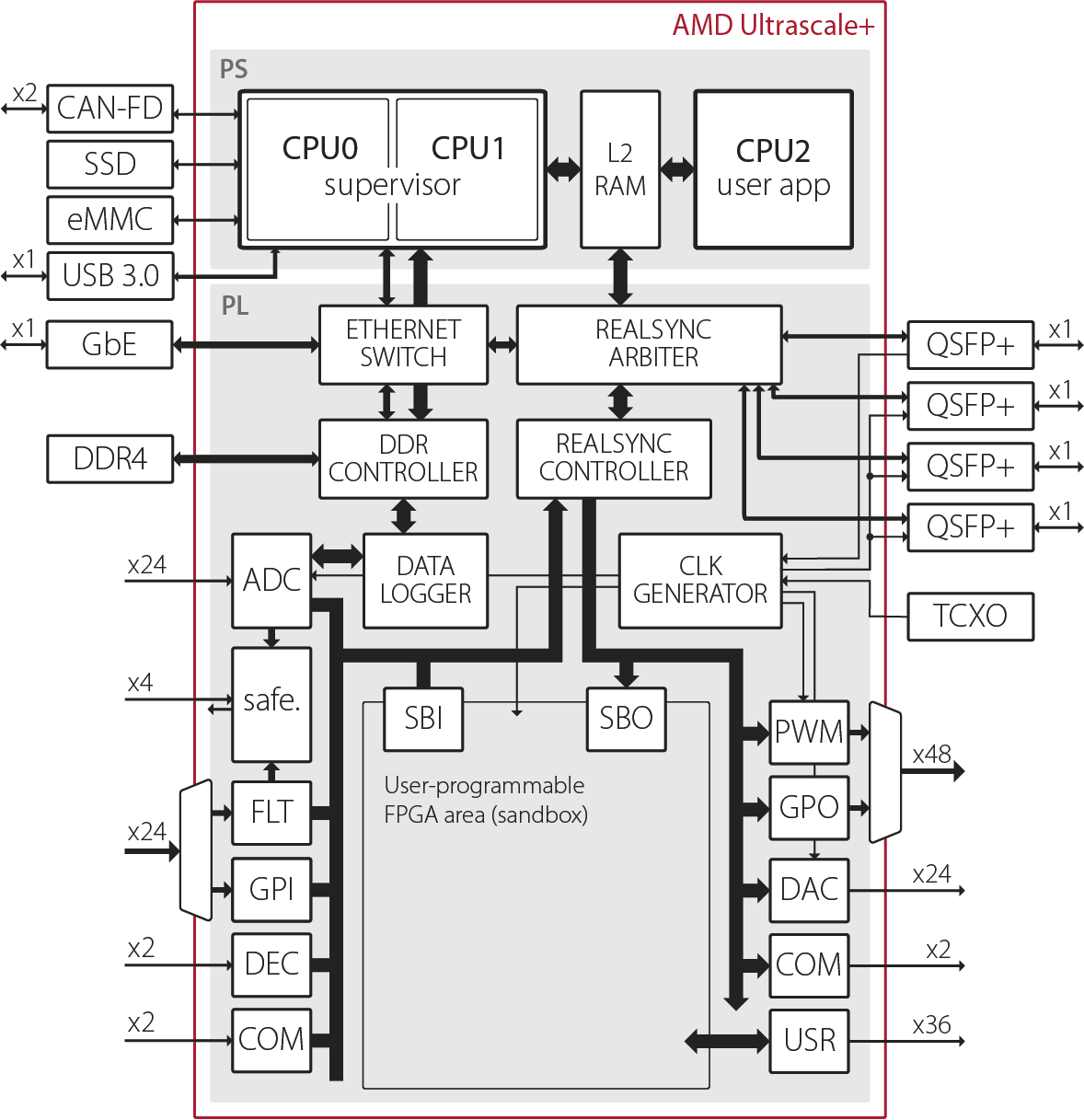
Firmware architecture of the B-Box 4 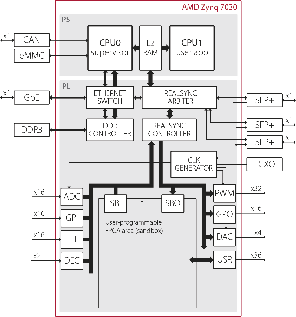
Firmware architecture of the B-Box 3
Beyond the architecture, the AMD Ultrascale+ present inside the B-Box 4 yields superior overall performance and a higher I/O count. A more general comparison of the devices is provided in PN250.
| Gen. 4 | Gen. 3 | ||||
|---|---|---|---|---|---|
| Controller | B-Box 4 | B-Box 3 | B-Box Micro | B-Board PRO | TPI8032 |
| SoC | Ultrascale+ | Zynq 7030 | |||
| CPU (PS) | 4xA53 / 1.5 GHz | 2xA9 / 1.0 GHz | |||
| FPGA (PL) | Kintex US 504K | Kintex 7 125K | |||
Key features
The digital control of power electronic systems is a hard real-time application, where insufficient determinism may lead to severe consequences, such as improper PWM outputs and even damage to the power stage. Furthermore, the total control delay, measured from the ADC sampling instant to the PWM update instant, is the cornerstone of achievable closed-loop control performance (bandwidth and stability margins).
Consequently, imperix controllers are purpose-built to simultaneously minimize that delay and guarantee that it remains rigorously constant (very low jitter). To achieve market-leading performance, the following aspects have received particular attention:
- No pipelining is used. In other words, the k-th control period uses data acquired immediately before (not at the k-1 period or earlier), and impacts the modulation parameters immediately afterward (not at the k+1 period or later). This differs from general-purpose RCP systems or HIL simulators, which commonly use pipelining to increase the achievable refresh rate at the cost of latency.
- Special management of timings. Control is tightly synchronized with sampling and modulation, using hardware-based interrupts generated by a high-quality time source. This also extends to networked control configurations, thanks to RealSync.
Underlying motivations
Such Systems on Chip (SoC) are very well suited for power electronics, thanks to the following reasons:
- The data volume involved with each control interrupt is relatively small, typically a few tens to hundreds of Bytes. However, the total input-to-output latency is critical. On SoCs, since the CPU and FPGA share the same die, the FPGA has direct access to the CPU cache, ensuring maximum throughput and virtually zero latency. This vastly overcompensates for the reduced CPU clock speed compared to the x86 architecture, especially for systems bottlenecked by the high latency of the PCIe bus (0.5-1.5us, typically).
- Power converters require simultaneous interfacing with multiple peripherals (ADCs, PWMs, etc.) and parallel processing of multi-channel data, both of which the FPGA handles effortlessly.
- Multi-core systems are well suited to properly isolate the execution of user-developed control algorithms from other communication- or supervision-related tasks. Notably, imperix controllers execute user code as a bare-metal application with strictly enforced real-time constraints. This is virtually impossible on x86 processors, which are too complex for bare-metal implementation.
Main data paths
All imperix controllers present two main data paths:
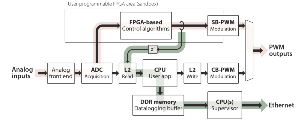
- CPU control path: Piloted by the user application CPU, this path is dedicated to data relevant for the user-implemented control algorithms. It does not involve large amounts of data but requires utmost priority, no pipelining, and minimal latency.
- Datalogging path: Piloted by the supervisor CPU(s), this path is dedicated to data monitoring and visualization in Cockpit. It runs fully independently and in parallel to the CPU control path. Various data streams are relevant:
- User variables: Global variables in user code can be logged from the user CPU and transferred to the supervisor CPU, at the control interrupt rate. This transfer occurs concurrently with the CPU-to-FPGA write cycle, as detailed in PN261.
- Oversampled analog data (B-Box 4 only): Raw ADC data are continuously sampled at the full acquisition speed (20Msps), acquired, and directly written to DDR memory. This way, the supervisor CPU can collect relevant data afterward, enabling their visualization in Cockpit.
- Digital I/O states (B-Box 4 only): PWM outputs and similar digital I/O signals are logged at 250 Msps, encoded (compressed), and written in a manner similar to DDR. This makes those signals also available for monitoring and troubleshooting, perfectly synchronized with ADC data.

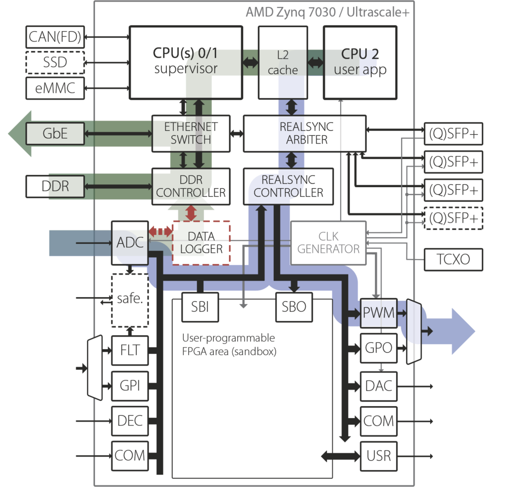
Other specialized data paths are also present:
- The protection path instantly blocks all PWM outputs when any undesirable or potentially dangerous event is detected, such as an out-of-range value on an analog input signal. At the FPGA level, all fault sources are routed to a fault manager, which monitors the system’s operating state and controls the PWM outputs. More information on the hardware protections is provided in PN263. At the software and user interface levels, faults affect the core state and can be back-traced using Cockpit’s log messages.
- Various custom data paths can be implemented in the user-programmable FPGA area. Some examples are shown below.
Firmware architecture
Along the CPU control path, three key subsystems are present:
- Data acquisition is best illustrated by the acquisition of analog signals, but more generally encompasses all the tasks related to retrieving measurements from physical sensors and making that data available to the CPU.
- CPU processing involves executing algorithms to determine appropriate control actions based on the acquired data. In most cases, these algorithms compute duty cycles (or similar modulation parameters) that are subsequently transferred to the modulators.
- Pulse-width modulation converts continuously valued modulation indices into binary gating signals using one or more configurable carriers. In most cases, conventional two-level carrier-based pulse-width modulation (PWM) is used, but other types of modulation are also possible. By extension, most of what applies to this block also applies to other output peripherals, such as analog outputs, digital outputs, etc.
The corresponding hardware resources are detailed below. Other FPGA-based peripherals are introduced later in this document. More information on the sequential treatment of data along the CPU control path is also provided in PN261.
Data acquisition
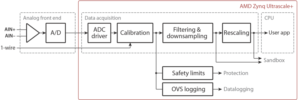
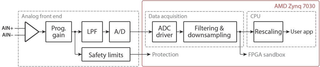
This subsystem is certainly where the various imperix controllers differ most. Among them, two fundamentally different approaches are used, exemplified by the B-Box 3 and 4 controllers:
- The B-Box 3 is designed to sample at a configurable rate (the CPU rate, up to 500 ksps), synchronously with the modulation (synchronous sampling, see PN258). Its analog front-end is hence shaped accordingly, offering comparable analog bandwidth. For users interested in implementing anti-alias filtering, programmable low-pass filters are available before sampling, i.e. at the analog level, before ADCs.
- The B-Box 4 is designed to always sample at a fixed rate of 20 Msps. Thanks to that, its analog front-end can provide effective anti-alias filtering without being configurable. However, configurable low-pass filtering is then required in the digital domain before the data is downsampled to the CPU rate. Ultimately, this yields the same result, but with the added benefit of fast-sampled data being available for monitoring.
The equivalent functional diagrams are shown below:
Other controllers implement a somewhat hybrid approach. The TPI8032, the B-Box micro, and the bare B-Board 3 (PRO) do not possess programmable low-pass filters. However, they can either sample at a user-configurable rate using synchronous sampling (without anti-aliasing filtering) or use Imperix’s proprietary synchronous averaging approach to achieve the devices’ maximum sampling rate of 2Msps and benefit from the averaging’s low-pass characteristic. More information on the commonly used sampling techniques in power electronics is available in PN258.
These architectures nonetheless possess the following common sub-elements:
- Analog front-end: Processes analog input signals to reject common-mode and RF perturbations before the useful signals reach the analog-to-digital converters (ADCs).
- ADC driver: Interfaces with physical ADCs to retrieve measurement data. The corresponding FPGA-based ADC driver defines the exact sampling instant. Specific to the B-Box 4, a calibration stage is also included (see PN255 for more information).
- Filtering and/or down-sampling: Applies configurable anti-alias filters and resamples the captured data down to the CPU control rate (see below for more details).
- Rescaling: Converts the raw integer ADC values into meaningful floating-point quantities in physical units (e.g. Amperes, Volts) before their transfer to the user app.
CPU processing
Data exchange between the PS and PL sections is performed over the SoC’s low-latency interconnect. In practice, the FPGA directly reads or writes data to the CPU’s DDR memory and L2 cache. On the other side of that memory, the user application CPU operates exclusively between the read and write caches, with no task other than processing control-relevant data.
The read cache contains a single data page with inbound data from the sensors. Transfers to this cache are scheduled and handled by the FPGA so that data arrive just before the CPU interrupt begins. Reciprocally, the write cache contains a single data page containing actuator output data. Transfers from this cache are triggered by the CPU at the end of its processing. These transfers typically take 20-100ns in single-controller applications, and can take up to 1-2 microseconds in a large control network with thousands of I/Os. Architecturally, the read and write buses are independent, allowing transfers to occur simultaneously (full-duplex).
In multi-controller configurations, more time is available between the end-of-conversion flag and the CPU interrupt, allowing all sensor data to be aggregated and transferred to the master in a timely manner. The same applies to actual data. Thanks to imperix’s proprietary tree-shaped networked control topology, transfers from slaves are initiated simultaneously, which vastly reduces latency. More information on data transfers over RealSync is available on the dedicated page.
Inbound sensor data
The control-relevant data received by the CPU is typically organized as shown below. One such table exists for each FPGA, whether it is physically located within the same controller or in a slave.
| FPGA peripheral | Gen. 4 (B-Box 4 only) | Gen. 3 (all others) | Remark |
|---|---|---|---|
| ADC | #channels x 32 bits | #channels x 16 bits | |
| DEC | #modules x 16 bits | #modules x 16 bits | |
| GPI | 1x 32 bits | 1x 16 bits | |
| FLT | 1x 16 bits | Also processed by safety | |
| COM (SSI/BiSS-C/EnDat) | 12x #ports x16 bits | 12x #ports x16 bits | |
| System overhead | 7x 16 bits | 7x 16 bits | |
| Total | Typ. 15-35x 32 bits | Typ. 15-40x 16 bits |
Outbound actuator data
The control-relevant data produced by the CPU is typically organized as shown below. One such table exists for each FPGA, whether it is physically located in the same controller or in a slave.
| FPGA peripheral | Gen. 4 (B-Box 4 only) | Gen. 3 (all others) | Remark |
|---|---|---|---|
| CB-PWM | 1-2x #channels x 32 bits | 1-2x #channels x 16 bits | +1 reg./ch with activate |
| SV-PWM | 3-6x #mod. x 32 bits (2L) 6-12x #mod. x 32 bits (3L) | 3-6x #mod. x 16 bits (2L) 6-12x #mod. x 16 bits (3L) | +3 registers with activate |
| SS-PWM | 2x #arms x 16 bits | 2x #arms x 16 bits | +1 register with activate |
| PP-PWM | 1x #angles x 16 bits 3x #modulators x 16bits | 1x #angles x 16 bits 3x #modulators x 16bits | +1 register with activate |
| DO-PWM | 1x #channels x 16 bits | 1x #channels x 16 bits | +1 register with activate |
| DAC | # channels x 16 bits | # channels x 16 bits | |
| GPO | 1-3x 16 bits | 1-2x 16 bits | |
| System overhead | 6x 16 bits | 6x 16 bits | |
| Total | Typ. 5-100x 32 bits | Typ. 5-80x 16 bits |
Modulation
Imperix controllers feature a powerful modulation subsystem that is nearly identical across all controller types. Its architecture is shown below. Its key functions include:
- PWM modulators: Represent the core of the gate signal generation. Multiple commonly used strategies are supported. Customizing PWM modulators in the sandbox area (SB-PWM) for specialized applications is also possible (an example is shown in PN127).
- Deadtime generator: Automatically inserts a configurable dead time between complementary PWM outputs to prevent shoot-through.
- High-resolution output (B-Box 4 only): Enables fine-tuning of the duty cycle or carrier phase shift with 250 ps resolution.
- Protection and activation: Authorizes or blocks the physical generation of PWM outputs:
- Activation: Provides independent control per PWM channel, controlled by the user code.
- Protection: Controlled by the core state machine, disables all PWM outputs in the event of a fault.
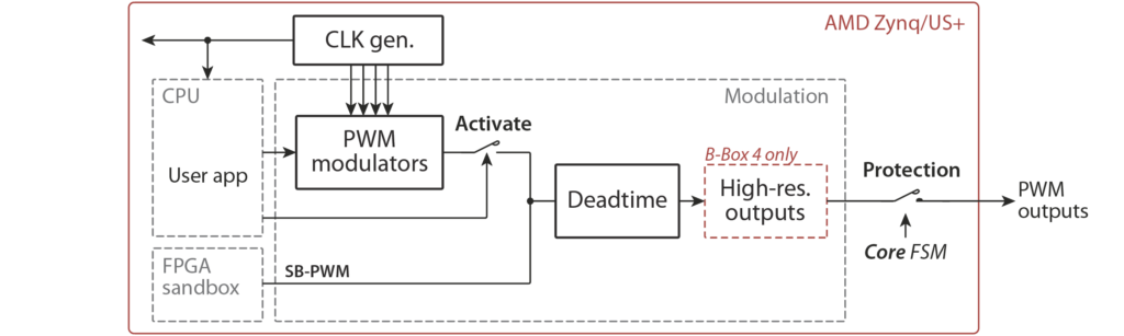
More information on the difference between the activation and protection mechanisms is given in PN138. Further details on the hardware protection mechanisms are also provided in PN263.
Timings management
A fourth fundamental block is the clock generation system, which is at the heart of imperix’s highly deterministic timings, low-latency operation, and ultra-precise synchronization.
Unlike microcontrollers, which conventionally manage the timing of acquisition, processing, and modulation using a cascade of interrupts, imperix controllers are clocked by a single resource, the CLK generator, and use predetermined relative phase shifts for each FPGA-based peripheral. This yields perfectly equivalent capabilities while significantly reducing latency, enabling advanced sampling approaches (see PN258), and supporting distributed modulation.
Imperix controllers provide 4 clocks (CLK0-CLK3) as timebases for all timing-critical tasks, such as ADC, PWM, and CPU interrupts. These clocks are derived directly from the 250 MHz FPGA main clock, which itself is produced from a very clean and stable timing source.
Among the four available clocks, CLK0 plays a special role, as it is used for all sampling- and processing-related events. As such, its frequency cannot be changed after code initialization, ensuring regular sampling. Two important internal clocks are derived from it, namely:
- SCLK, the physical sampling clock. It runs at the same rate as CLK0, but with a user-defined constant phase shift that sets the exact sampling instant. This also defines the rate at which data can be made available inside the FPGA sandbox.
- The CPU interrupt clock, which triggers the execution of the control task. When required, it can be obtained by decimating SCLK with a postscaler.
CLK1, CLK2, and CLK3 are optional clocks that can be configured to run at variable frequencies. These clocks are typically used in applications where the sampling frequency and PWM carrier frequency differ (e.g., double-rate PWM updates, see PN259), or where the modulation uses a variable-frequency carrier (e.g., with resonant converters).
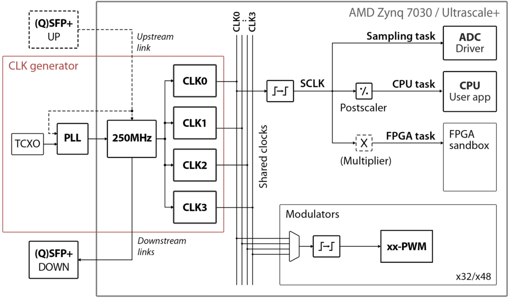
Thanks to imperix’s RealSync technology, the clock domain derived from the master’s 250MHz base clock is distributed across the network, enabling the synchronization of all four shared clocks with an absolute frequency matching and a phase accuracy of ±2ns. In other words, from a timing perspective, all FPGA-based peripherals behave as if they belonged to the same physical SoC.
Practical considerations about the timing configuration for imperix controllers are documented in PN259..
Frequency domains derived from CLK0
As presented above, CLK0 serves as the reference clock for several acquisition- and processing-related mechanisms. At the hardware level, this defines several frequency domains:
- Oversampling domain FOVS (B-Box 4 only), representing the physical sampling frequency. Since this frequency is fixed (20Msps), CLK0 and SCLK are constrained to be an integer sub-multiple of 20 MHz.
- User sampling domain FSCLK, corresponding to the CLK0 frequency, but with a user-configurable sampling phase. Custom logic in the FPGA sandbox can access ADC data at this rate. Therefore, the execution rate of custom FPGA control tasks is usually identical to FSCLK.
- CPU frequency domain FCPU, setting the execution rate for the CPU-based control tasks. By default, FCPU equals FSCLK. However, it can optionally be slowed down by adding a postscaler, which is typically useful to allow faster tasks to run on the FPGA.
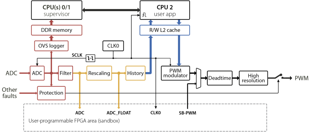
The typical achievable rates are summarized in the table below.
| FOVS | FSCLK | FCPU | FFPGA | |
|---|---|---|---|---|
| B-Box 4 | 20 MHz | 50 Hz – 10 MHz | 50 Hz – 500 kHz | 50 Hz – 10 MHz |
| B-Box 3 | N/A | 50 Hz – 500 kHz | 50 Hz – 200 kHz | 50 Hz – 500 kHz |
| B-Board / B-Box Micro / TPI8032 | N/A | 50 Hz – 2 MHz | 50 Hz – 200 kHz | 50 Hz – 2 MHz |
Other FPGA-based peripherals
In addition to the acquisition (ADC) and modulation (PWM) resources presented above, several other subsystems are implemented as FPGA-based peripherals. All these resources are accessible using two different register types:
- Configuration registers are designed to receive information that is written only at startup or updated rarely during operation. Typical examples include the configuration of the low-pass filters, the CPU interrupt rate, or the PWM dead time. Writing to (or reading from) configuration registers uses RealSync’s read-through (or write-through) traffic, which occurs immediately after the corresponding function call in the software.
- Real-time registers are systematically read or written once per CPU interrupt, even if the related information has not changed during the interval. This uses RealSync read-back (or write-back) traffic, which is scheduled together with all other read (respectively write) instructions before (respectively after) the execution of the CPU interrupt.
Other than to the ADC and PWM resources, this applies to:
Input peripherals
- FLT: These are special-purpose digital inputs that are directly tied to the internal fault manager. They can be used to react to protection-related signals faster than the CPU rate.
- GPI: The corresponding pins are general-purpose digital inputs that can be read by user code at the CPU rate or via the FPGA sandbox (faster). On the B-Box 4, more pins are available than on Gen. 3 controllers, but these pins are multiplexed with FLT inputs.
- DEC: These inputs can be configured as either four independent or two differential decoders for quadrature-encoded signals. This is typically used by analog motor speed/position sensors. The corresponding pins are also multiplexed with GPI pins on all controllers.
- COM: Two ports are available to support serial communication from digital encoders using EnDat 2.2, SSI, or BiSS-C. This peripheral is only available on the B-Box 4.
The values read or decoded by input peripherals are latched synchronously with SCLK. However, a few differences must be noticed regarding the relative phase:
- The angle captured by the DEC peripheral is always latched synchronously with the ADC data, specifically at the rising edge of SCLK.
- GPI and FLT inputs are always latched as late as possible before the CPU read transfer. In practice, latching occurs simultaneously with the ADC end-of-conversion flag.
- Data transfers from digital encoders (COM peripheral) are initiated by SCLK, but the corresponding data can be retrieved only on a subsequent SCLK edge. If time permits, the corresponding measurement will be available in the next cycle. Otherwise, a two-period delay is induced, and rate decimation occurs.
Output peripherals
- DAC: Digital-to-analog converter (DAC) outputs are peripherals specific to the B-Boxes 3 and 4. Their implementation, I/O count, and performance differ significantly.
- GPO: The corresponding pins are general-purpose digital outputs that can be asserted by the CPU or directly from the sandbox (faster). On the B-Box 4, more pins are available than on Gen. 3 controllers, but these pins are multiplexed with PWM outputs.
- COM: Serial communication to digital encoders (as opposed to from them) is technically possible using EnDat 2.2. This is, however, not (yet) supported at the software level.
For output peripherals, the exact instant of their update depends on the peripheral type:
- CB-PWM and SS-PWM have their update instant defined by the CLK they are tied to (CLK0–CLK3), the carrier type, and whether single- or double-update rate is implemented. This is generally independent of CPU operation, except when all peripherals are clocked on CLK0.
- SV-PWM resources update their outputs identically to CB-PWM, using triangular carriers and single- or double-rate update.
- DO-PWM and GPOs are latched immediately at the end of the CPU write cycle.
- DAC data are transmitted to the physical DAC circuits at the end of the write cycle, and their outputs are latched immediately afterward. The total update latency is 2.26 µs across all devices.
FPGA sandbox
The programmable logic (PL) section of the SoC is partitioned into two areas:
- Uneditable firmware area: Contains all the logic required to implement and communicate with the FPGA-based peripherals. This is encapsulated in a base firmware IP that must always be present. For FPGA users, this IP can be customized (wizard) and instantiated within the FPGA sandbox, allowing custom logic to be implemented around it. More information is available in the IP product guide.
- User-programmable area (sandbox): The remaining resources are available for users to develop their own logic, providing maximum flexibility for advanced applications. The user-programmable area represents 50-75% of the total logic resources in both Gen. 3 and Gen. 4 controllers. Getting-started information for FPGA-based development is also available in PN159.
Thanks to the flexibility of the SoC architecture, users can also combine FPGA and CPU resources for more complex, hybrid applications:
- High-performance control: Typically, users leverage the FPGA sandbox to implement algorithms that run significantly faster on FPGA than on CPU. For example, TN147 demonstrates an FPGA-based current controller for a grid-following inverter running at 650 kHz on Gen. 3 hardware. In such a case, the CPU is used only indirectly to monitor variables using SBI blocks. The corresponding paths are illustrated below:
- Multi-rate control: In this case, both the FPGA and the CPU are used for control-relevant purposes but operate at decoupled rates. For example, in cascaded controllers, a typical practice is to run a high-speed inner loop (e.g., current control) in the FPGA, while the CPU manages the slower outer loop (e.g., voltage or speed control).
- Interface with custom peripherals: The FPGA can also interface with custom hardware peripherals, for instance, via the dedicated USR pins. Typical examples include:
Communication resources
Various means of communication are available and can be used either across imperix controllers or with third-party devices. The corresponding protocols are listed below and further documented in PN202.
| Gen. 4 (B-Box 4) | Gen. 3 (all others) | |
|---|---|---|
| CAN | CAN-FD (2x) | CAN (1x) |
| Ethernet | TCP/IP, Modbus TCP, OPC-UA | TCP/IP, Modbus TCP, OPC-UA |
| RealSync | 4x QSFP+ (40Gbps) | 3x SFP+ (10Gbps) N/A on B-Box micro |
| Serial COM (RS-232, RS-485) | BiSS-C, EnDat, SSI | N/A |
At the hardware level, these protocols are supported in different manners and serve distinct purposes. This directly relates to their achievable performance:
- CAN(-FD) is supported from the supervisor CPU(s) in the PS section of the SoC. The corresponding read data is made available in the L2 shared cache before the CPU interrupt begins. Respectively, write data is extracted from the cache after the CPU interrupt ends. The resulting latencies are negligible given that CAN is a slow and non-deterministic protocol.
- Ethernet is used for various means:
- User-configurable communication tasks can be implemented using UDP or Modbus TCP. These are supported similarly to CAN(-FD), via the supervisor CPU(s). Given the slow and non-deterministic latencies of these protocols, this is also adequate.
- Device support tasks primarily include device programming and monitoring via Cockpit, which uses OPC UA over TCP/IP. To guarantee optimal performance when extracting data from DDR memory or bridging device-to-device Ethernet communication over RealSync, a Gigabit-capable Ethernet switch is implemented in the FPGA fabric. The related resources are neither visible nor editable by the user.
- RealSync also supports various duties:
- Clock dissemination: The 250 MHz base clock issued by the network top master is automatically disseminated throughout the control network. This is subsequently used to reconstruct and align the CLK0-CLK3 clocks across all devices. The corresponding method is a patended imperix technology.
- Master-slave communication: The CPU read and write cycles are arranged and scheduled so that data from all devices is written (or read) into the L2 cache right before (or after) the CPU interrupt. This uses automatically-configured read- or write-back traffic that guarantees minimal latency.
- Master-master communication: For CPU-to-CPU communication, i.e. for communication between user codes, SFP blocks can be instantiated to “manually” arrange data transfers. This uses write-through traffic, resulting in a 1-period latency for concurrently scheduled CPU events.
- Ethernet encapsulation: To enable Cockpit to communicate with slaves, Ethernet can be carried over RealSync as an encapsulated, low-priority traffic. This simplifies connectivity for the user and also leverages the fiber’s galvanic isolation. In this context, the RealSync arbiter has the critical task of guaranteeing the absolute, latency-free, priority of hard real-time traffic over Ethernet traffic.
- Serial communication (COM) with incremental encoders is supported in the same way as other FPGA-based I/O peripherals. However, because the duration of data transmission is sensor-dependent, variable delays occur (see above).
To go further
The following pages can help learn more about how imperix controllers operate:
 By Shu Wang • July 7, 2026 • PN263
 By Nicolas Cherix • July 7, 2026 • PN261
 By Julien Orsinger • September 20, 2022 • PN138