Table of Contents
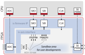
The Sandbox Output towards FPGA (SBO) block writes the value of the SBO registers in the FPGA. It is used to transfer data from the CPU to the user-made code within the FPGA. To transfer data from user-made code within the FPGA to the CPU, the SBI block should be used.
An SBO register can be configured as:
- a configuration register: the value is written only once, at the code launch
- a real-time register: the value can change anytime during the control
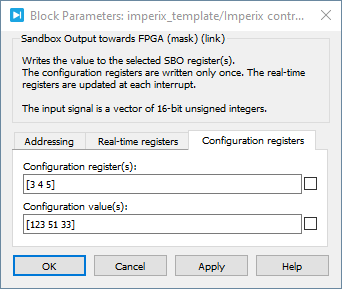
In Simulink and PLECS, configuration register values are defined from the block mask and real-time registers from the block input signal.
Information on FPGA edition is available on:
Usage examples of the SBI block are available on:
- FPGA-based hysteresis current control (TN120)
- FPGA-based SPI communication IP for A/D converter (TN130)
- FPGA-based direct torque control using Vivado HLS (TN133)
Simulink block
Signal specification
The input expects a vector of 16-bit unsigned integer values to write to the SBO registers.
Up to 8 real-time registers and 8 configuration registers can be written from a single SBO block. Multiple SBO blocks can be used to write to more registers.
Parameters
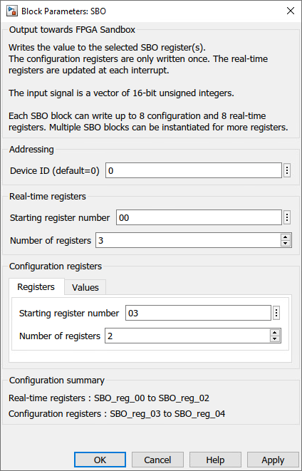
Device IDselects which B-Box/B-Board to address when used in a multi-device configuration.- Real-time registers:
Starting register numberandNumber of registersdefine the range of registers to write to. - Configuration registers:
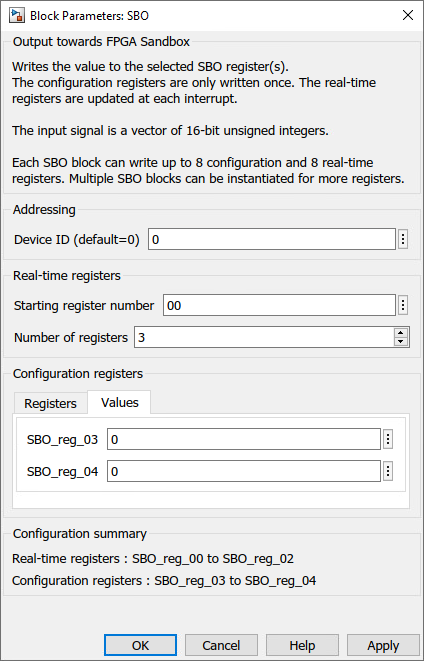
Starting register numberandNumber of registersdefine the range of registers to write to. Their values can be set from theValuestab.
PLECS block
Signal specification
Parameters
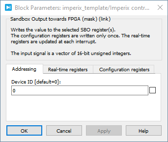
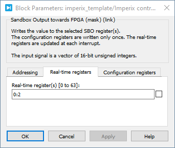
Device IDselects which B-Box/B-Board to address when used in a multi-device configuration.Real-time register(s)(vectorizable) defines the real-time registers to write to using the input signalConfiguration register(s)(vectorizable) defines the configuration registers to write to andConfiguration values(s)(vectorizable) sets their constant values.


