Table of Contents
This note provides step-by-step guidance to create a Xilinx Vivado project, add customized logic, generate a bitstream, and load it into the B-Box/B-Board.
The required software and sources files are:
- Vivado HL Design Suite (available for free as the WebPACK edition)
- Sandbox sources
– PN168: Xilinx Vivado Design Suite installation
– PN159: Getting started with FPGA control development
Software resources
Installing Vivado SDK
A Xilinx account is needed to download and install the Vivado SDK. It can be created by following the link https://www.xilinx.com/registration/create-account.html.
- Go to Xilinx download page: https://www.xilinx.com/support/download/index.html/content/xilinx/en/downloadNav/vivado-design-tools.html
- Download the installer. (for the free Windows version select ” Vivado HLx: WebPACK and Editions”)
- Run the downloaded file
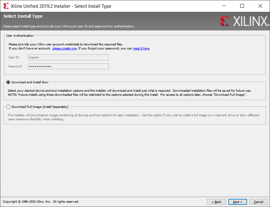
- Enter your login credentials and select Download and Install Now
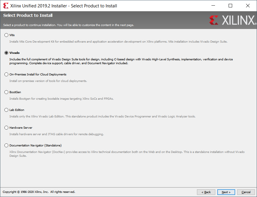
1. Select Vivado
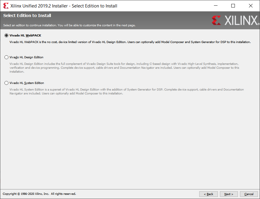
2. Select Vivado HL WebPACK
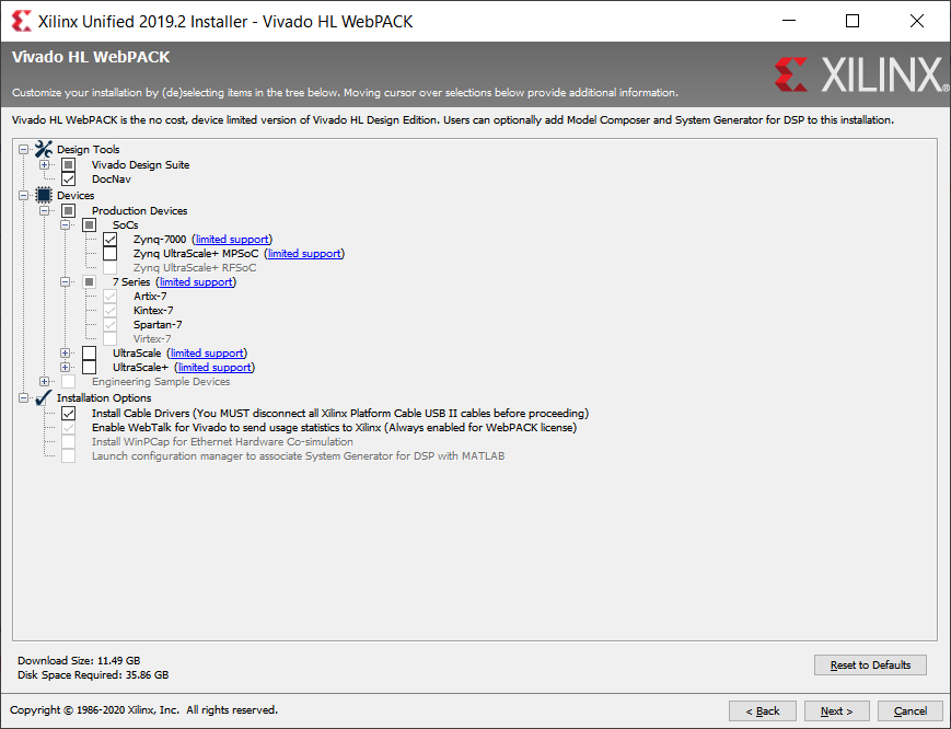
3. The only mandatory item is Zynq-7000 support
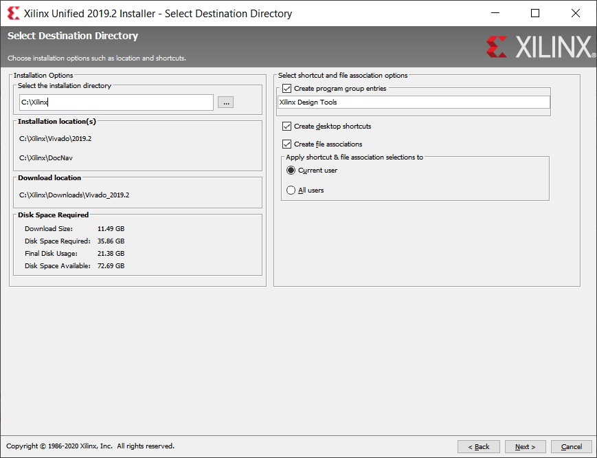
4. We recommend keeping the default installation directory
5. Hit Install
Creating a sandbox template project
Download the required sources to use the sandbox:
- Download the archive sandbox_sources_3.x_xxxx.x.zip from imperix’s website, under Support → Downloads (https://imperix.com/downloads)
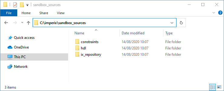
- Unzip it and save the content somewhere on your PC, for instance in
C:\imperix\.
To create a sandbox project:
- Open Vivado
- Click Create Project
- Chose a name and a location.
- Select project type RTL Project and check the box Do not specify sources at this time.
- Select the part xc7z030fbg676-3.
- Hit Finish. The project should open.
- In Settings, the preferred Target Language can be set (VHDL or Verilog).
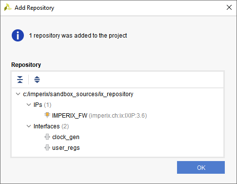
- Go to the IP Catalog, right-click on Vivado Repository, hit Add repository…
SelectC:/imperix/sandbox_sources/ix_repository/.
The IMPERIX_FW IP, clock_gen, and user_regs interfaces should be found.
- Click on Create block design, name it “top” and click OK
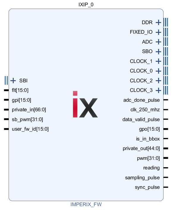
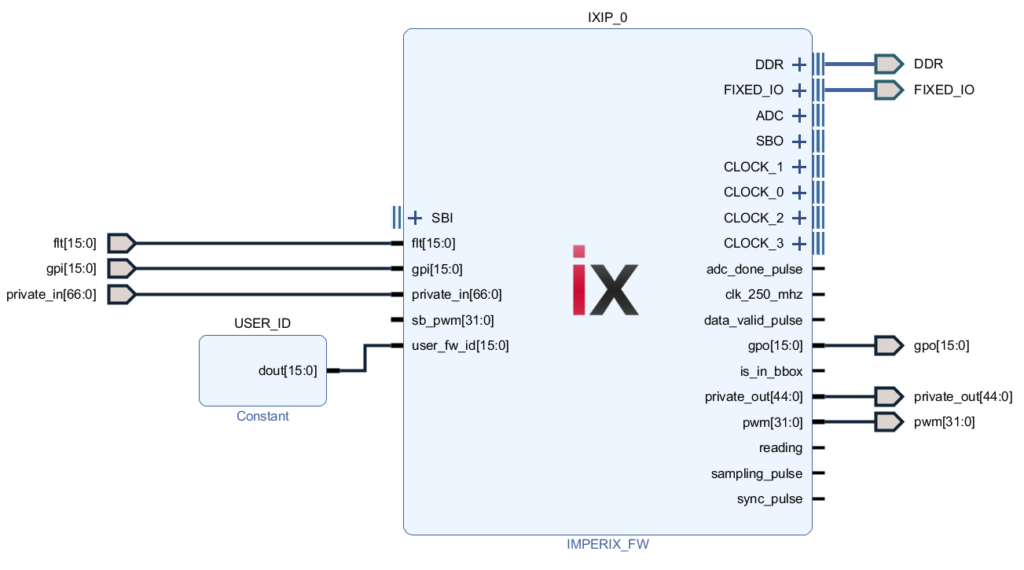
- Open the freshly created block design, do a right-click, select Add IP… and search for “IMPERIX_FW” and hit ENTER.
- Keep the [Ctrl] key pressed and select the IP pins
flt,gpi,private_in,DDR,FIXED_IO,gpo,pwmandprivate_out.
Hit [Ctrl+T] to create top-level ports. - Remove the “_0” from every port name generated. For instance “
flt_0[15:0]” becomes “flt[15:0]“. - The
user_fw_idinput may be used to identify the firmware version. We recommend instantiating a Constant IP (Right-click, Add IP…, search for Constant) to give an identification number to the design.
- Go to the Sources tab, right-click on the block design file (top.bd) and select Create HDL Wrapper…
In the dialog box choose Let Vivado manager wrapper and auto-update and hit OK. - Right-click on Design Sources folder
Choose Add Sources…
Check Add or create constraint
Click on Add Files
SelectC:/imperix/sandbox_sources/constraints/sandbox_pins.xdc
Uncheck Copy sources into the project
Hit Finish
From this point the project is synthesizable. The next chapter covers how to add custom logic to the design.
Information on how to use the imperix firmware IP can be found in the product note about editing the FPGA firmware.
Adding custom logic to the sandbox project
The following steps use the file sandbox_template.vhd as an example to illustrate how to add a VHDL entity to the project and interface it to the imperix firmware IP.
- Right-click on Design Sources and choose Add Sources…. Check Add or create design sources.
- Select
imperix_sandbox_sources/hdl/sandbox_template.vhd.
We recommend unchecking “Copy sources into project” and working directly from the files in the folderimperix_sandbox_sources/hdl/so the sources can be shared across multiple projects. - Right-click somewhere in the block design and chose Add module… Select the SandboxTemplate module. Alternatively, you can drag the file listed in the Design Sources and drop it on your diagram.
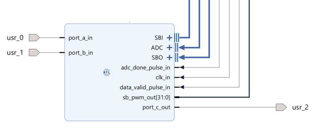
- Connect the pins as follows:
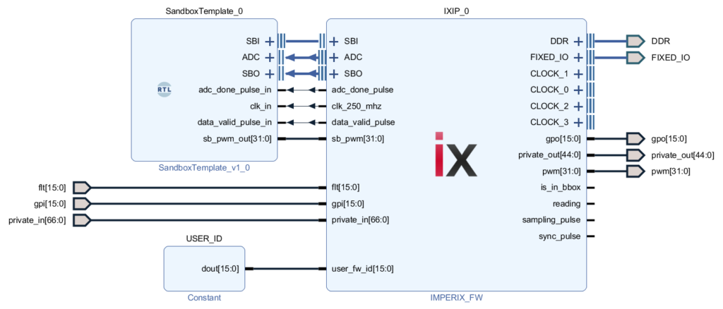
The imperix firmware IP provides 64 SBI registers, 64 SBO registers, and 24 ADC registers which are grouped in interfaces for better readability. The sandbox_template.vhd illustrates how to use X_INTERFACE_INFO attributes to infer the ADC, SBI, and SBO interfaces.
library IEEE;
use IEEE.STD_LOGIC_1164.ALL;
use IEEE.NUMERIC_STD.ALL;

entity SandboxTemplate is
  Port (

    -- Analog-to-digital conversion results in 2's complement format
    adc_00_in : in std_logic_vector(15 downto 0) := (others => '0');
    adc_01_in : in std_logic_vector(15 downto 0) := (others => '0');
    adc_02_in : in std_logic_vector(15 downto 0) := (others => '0');
    adc_03_in : in std_logic_vector(15 downto 0) := (others => '0');
    adc_04_in : in std_logic_vector(15 downto 0) := (others => '0');
    adc_05_in : in std_logic_vector(15 downto 0) := (others => '0');
    adc_06_in : in std_logic_vector(15 downto 0) := (others => '0');
    adc_07_in : in std_logic_vector(15 downto 0) := (others => '0');
    adc_08_in : in std_logic_vector(15 downto 0) := (others => '0');
    adc_09_in : in std_logic_vector(15 downto 0) := (others => '0');
    adc_10_in : in std_logic_vector(15 downto 0) := (others => '0');
    adc_11_in : in std_logic_vector(15 downto 0) := (others => '0');
    adc_12_in : in std_logic_vector(15 downto 0) := (others => '0');
    adc_13_in : in std_logic_vector(15 downto 0) := (others => '0');
    adc_14_in : in std_logic_vector(15 downto 0) := (others => '0');
    adc_15_in : in std_logic_vector(15 downto 0) := (others => '0');

    -- Output to the sandbox for CPU to FPGA communication
    sbo_reg_00_in : in std_logic_vector(15 downto 0) := (others => '0');
    sbo_reg_01_in : in std_logic_vector(15 downto 0) := (others => '0');
    sbo_reg_02_in : in std_logic_vector(15 downto 0) := (others => '0');
    -- you can add more registers here

    -- Timing pulses
    sampling_pulse_in : in std_logic;
    adc_done_pulse_in : in std_logic;
    read_pulse_in : in std_logic;
    data_valid_pulse_in : in std_logic;

    -- Sandbox PWM
    sb_pwm_out : out std_logic_vector(31 downto 0);

    -- Main clock running at 250 MHz
    clk_in : in std_logic
  );
end SandboxTemplate;

architecture impl of SandboxTemplate is

  ATTRIBUTE X_INTERFACE_INFO : STRING;
  ATTRIBUTE X_INTERFACE_PARAMETER : STRING;

  ATTRIBUTE X_INTERFACE_INFO of clk: SIGNAL is "xilinx.com:signal:clock:1.0 clk CLK";

  -- Informations to infer the SBI interface
  ATTRIBUTE X_INTERFACE_INFO of sbi_reg_00_out: SIGNAL is "imperix.ch:ix:user_regs_rtl:1.0 SBI reg_00";
  ATTRIBUTE X_INTERFACE_INFO of sbi_reg_01_out: SIGNAL is "imperix.ch:ix:user_regs_rtl:1.0 SBI reg_01";
  ATTRIBUTE X_INTERFACE_INFO of sbi_reg_02_out: SIGNAL is "imperix.ch:ix:user_regs_rtl:1.0 SBI reg_02";

  -- Informations to infer the SBO interface
  ATTRIBUTE X_INTERFACE_INFO of sbo_reg_00_in: SIGNAL is "imperix.ch:ix:user_regs_rtl:1.0 SBO reg_00";
  ATTRIBUTE X_INTERFACE_INFO of sbo_reg_01_in: SIGNAL is "imperix.ch:ix:user_regs_rtl:1.0 SBO reg_01";
  ATTRIBUTE X_INTERFACE_INFO of sbo_reg_02_in: SIGNAL is "imperix.ch:ix:user_regs_rtl:1.0 SBO reg_02";

  -- Informations to infer the ADC interface
  ATTRIBUTE X_INTERFACE_INFO of adc_00_in: SIGNAL is "imperix.ch:ix:user_regs_rtl:1.0 ADC reg_00";
  ATTRIBUTE X_INTERFACE_INFO of adc_01_in: SIGNAL is "imperix.ch:ix:user_regs_rtl:1.0 ADC reg_01";
  ATTRIBUTE X_INTERFACE_INFO of adc_02_in: SIGNAL is "imperix.ch:ix:user_regs_rtl:1.0 ADC reg_02";
  ATTRIBUTE X_INTERFACE_INFO of adc_03_in: SIGNAL is "imperix.ch:ix:user_regs_rtl:1.0 ADC reg_03";
  ATTRIBUTE X_INTERFACE_INFO of adc_04_in: SIGNAL is "imperix.ch:ix:user_regs_rtl:1.0 ADC reg_04";
  ATTRIBUTE X_INTERFACE_INFO of adc_05_in: SIGNAL is "imperix.ch:ix:user_regs_rtl:1.0 ADC reg_05";
  ATTRIBUTE X_INTERFACE_INFO of adc_06_in: SIGNAL is "imperix.ch:ix:user_regs_rtl:1.0 ADC reg_06";
  ATTRIBUTE X_INTERFACE_INFO of adc_07_in: SIGNAL is "imperix.ch:ix:user_regs_rtl:1.0 ADC reg_07";
  ATTRIBUTE X_INTERFACE_INFO of adc_08_in: SIGNAL is "imperix.ch:ix:user_regs_rtl:1.0 ADC reg_08";
  ATTRIBUTE X_INTERFACE_INFO of adc_09_in: SIGNAL is "imperix.ch:ix:user_regs_rtl:1.0 ADC reg_09";
  ATTRIBUTE X_INTERFACE_INFO of adc_10_in: SIGNAL is "imperix.ch:ix:user_regs_rtl:1.0 ADC reg_10";
  ATTRIBUTE X_INTERFACE_INFO of adc_11_in: SIGNAL is "imperix.ch:ix:user_regs_rtl:1.0 ADC reg_11";
  ATTRIBUTE X_INTERFACE_INFO of adc_12_in: SIGNAL is "imperix.ch:ix:user_regs_rtl:1.0 ADC reg_12";
  ATTRIBUTE X_INTERFACE_INFO of adc_13_in: SIGNAL is "imperix.ch:ix:user_regs_rtl:1.0 ADC reg_13";
  ATTRIBUTE X_INTERFACE_INFO of adc_14_in: SIGNAL is "imperix.ch:ix:user_regs_rtl:1.0 ADC reg_14";
  ATTRIBUTE X_INTERFACE_INFO of adc_15_in: SIGNAL is "imperix.ch:ix:user_regs_rtl:1.0 ADC reg_15";

begin

  sb_pwm_out <= (others => '0');

  sbi_reg_00_out <= (others => '0');
  sbi_reg_00_out <= (others => '0');
  sbi_reg_00_out <= (others => '0');

  MY_PROCESS : process(clk_in)
  begin
    if rising_edge(clk_in) then

      if adc_done_pulse_in = '1' then
        -- sampled value are available in ADC registers
      end if;

      if data_valid_pulse_in = '1' then
        -- new data has been written to SBO registers
      end if;

    end if;
  end process MY_PROCESS;

end impl; Code language: VHDL (vhdl)Using the USR pins
The file sandbox_pins.xdc contains the constraints for the 36 USR pins.
To use USR pins:
- un-comment the line of the pins to use
- create the corresponding ports in the Vivado block design (right click, Create Port…)
####
===========================================================================
#### USR
####
===========================================================================

set_property -dict {PACKAGE_PIN AE10 IOSTANDARD LVCMOS33} [get_ports {usr_0}]
set_property -dict {PACKAGE_PIN AF10 IOSTANDARD LVCMOS33} [get_ports {usr_1}]
set_property -dict {PACKAGE_PIN AE12 IOSTANDARD LVCMOS33} [get_ports {usr_2}]
#set_property -dict {PACKAGE_PIN AF12 IOSTANDARD LVCMOS33} [get_ports {usr_3}]
#set_property -dict {PACKAGE_PIN AE13 IOSTANDARD LVCMOS33} [get_ports {usr_4}]
#set_property -dict {PACKAGE_PIN AF13 IOSTANDARD LVCMOS33} [get_ports {usr_5}]
...Code language: Tcl (tcl)
Loading the bitstream into the device
Generate and export the bitstream:
- Click Generate bitstream. It will launch the synthesis, implementation and bitstream generation
- Click on File → Export → Export Bitstream File…
Using BB Control, the bitstream can be loaded using the following procedure:
- Go to the Configuration tab
- Click on the “import bitstream” button, it will upload the bitstream into the B-Board SD card
A check in the load at startup checkbox indicates that the device will load the imported customized bitstream at the next power-cycle instead of the standard one.
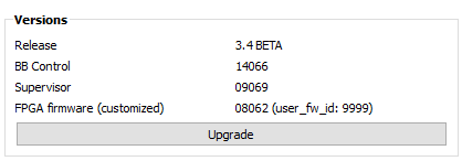
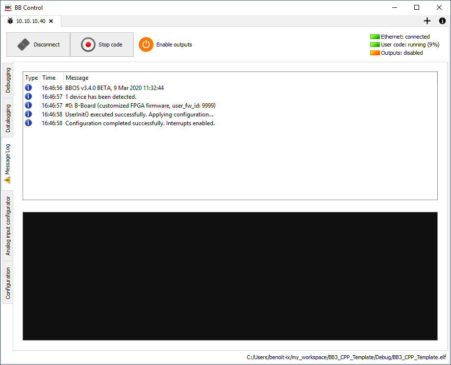
In the Versions section is indicated if the device has a customized bitstream loaded.
The information is also available from the Message Log.
Update the imperix firmware IP sources
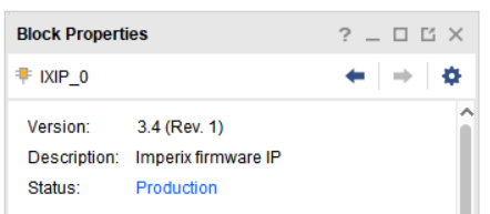
The version of the imperix IP currently in use is found in the block properties of the IP (by clicking on the IP)
To update the sources of the imperix IP
- Replace the sandbox sources by the ones of the targeted version.
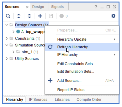
- Do a right click on Design Sources and click on Refresh Hierarchy
- An information message should appear, click on Refresh IP Catalog
- Finally, under the IP Status tab, select the IXIP and click Upgrade Selected


