Table of Contents
BB control has been discontinued in 2022. It has been replaced by Cockpit which offers an extended set of features and a superior user experience.
Cockpit is included in latest SDK, which is available from https://imperix.com/downloads/.
The BB Control Timing info tab provides a graphical representation of the various computation and communication delays involved in the B-Board PRO and B-Box RCP power electronics controllers during run-time.
It is particularly useful to observe the delays involved in the control dynamics of the system as explained in Identifying the discrete control delay (PN142) and adjust the control parameters accordingly, such as the \(K_p\) and \(K_i\) of a PI control implementation as shown in Basic PI control implementation (TN105).
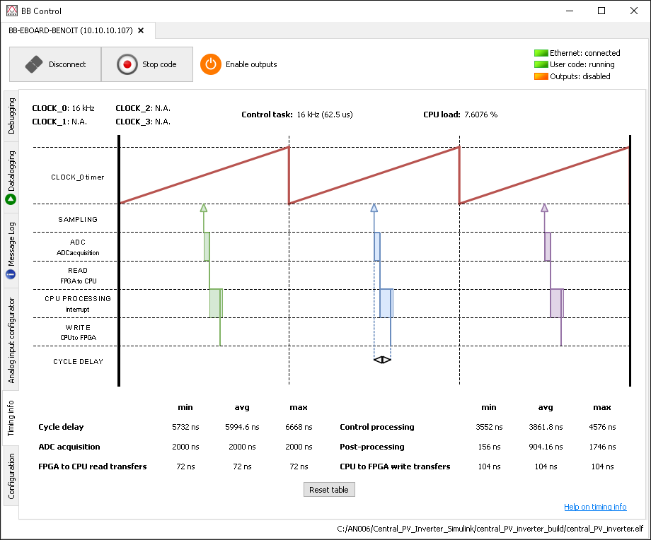
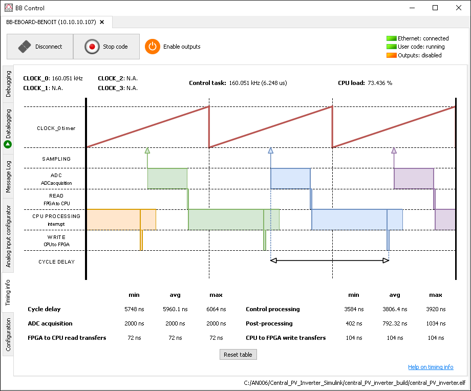
Below are screenshots of the Timing info tab when running the model Central PV inverter (AN006) in two scenarios.
Clock generators, control task routine, and CPU load
At the top of the window, the following information are shown:
CLOCK_0, CLOCK_1, CLOCK_2, and CLOCK_3 show the configured frequency of the 4 Clock generator.
The Control task routine execution frequency and period are also displayed. Note that the control task is always mapped on CLOCK_0.
The CPU load represents how much time the CPU spends in the interrupt routine. Safety mechanisms are implemented to detect CPU overload. An overload can result from a control algorithm too complex or an execution frequency too high.
The timing graph
The timing graph accurately represents the delays involved in the execution of the user control code.
CLOCK_0 timer represents the value of the clock generator counter. CLOCK_0 is used as the time-base for the sampling events and the control task routine execution. In most cases, the PWM modulators are also based on CLOCK_0.
SAMPLING shows the sampling events, i.e. the instants where the ADCs sample the input analog signals. In the example above, the sampling phase is set 0.5 so the sampling occurs in the middle of the period of the PWMs that are based on CLOCK_0.
ADC acquisition shows the delay between a sampling event and the availability of the values in the FPGA. It comprises the analog-to-digital delay and the results transfer to the FPGA delay. This value can be set to 2000 ns (B-Box RCP or B-Board PRO) or to 500 ns (B-Board PRO).
FPGA-to-CPU transfers are executed right after the ADC results are available in the FPGA. The values transferred are typically the ADC measurements, the GPI values, or the angle decoder output.
CPU PROCESSING shows the time the CPU spends executing the interrupt routine. To execute the CPU-to-FPGA transfers as early as possible (and reducing the overall response delay), the interrupt routine is separated into two phases:
- The control task execution is the delay to execute the user control model and update the modulation parameters and other FPGA values. The CPU-to-FPGA transfers are executed right after, in parallel with the post-processing execution.
- The post-processing execution is the delay necessary to perform all the tasks that are not directly involved in the control algorithm. It includes the datalogging execution, the CAN communication, the Simulink external mode execution, etc.
CPU-to-FPGA transfers are performed once the control task execution is over. The values transferred are typically the PWM modulation parameters (duty-cycle, phase), the GPO values, or the DAC values.
CYCLE DELAY represents the delay between the sampling event and when the newly computed data are available in FPGA (ADC acquisition + FPGA-to-CPU transfers + control task execution + CPU-to-FPGA transfers). This value can be used by the user to compute the control delay and the total loop delay, as explained in Identifying the discrete control delay (PN142).
The measurements table
The table at the bottom of the window provides the values used to generate the timing graph (avg), and a saves the min and max of each value. The reset table button resets the values of the table.
The ADC acquisition, the FPGA to CPU read transfers, and CPU to FPGA write transfers are fixed values computed at code launch.
The control processing and post-processing values are measured from the CPU using the CPU physical counter.
The cycle delay value is precisely measured directly from within the FPGA.


