Table of Contents
Model Composer is a Simulink add-on software developed by Xilinx. It is a high-level synthesis (HLS) tool that allows the user to program an FPGA-based algorithm without the need to write code. Thanks to this approach, behavioral simulations can be run prior to code generation, enabling engineers to validate the correctness of their FPGA design very early in the design process.
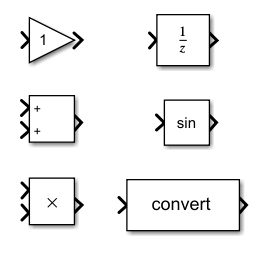
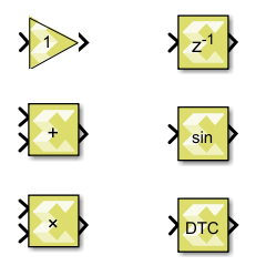
Since it is directly integrated within the Matlab Simulink environment, Model Composer is fairly easy to use for regular Simulink users. The provided blockset offers numerous elementary blocks and functions that strongly resemble existing Simulink blocks. Therefore, if users already have a CPU-based model available in Simulink, they can easily build an FPGA model by replacing the Simulink blocks with corresponding Model Composer blocks.
An alternative to Model Composer is Xilinx Vitis HLS, a tool that provides the same features but for C++ developers and that is free of charge. As a matter of fact, Model Composer uses Vitis HLS under the hood. Indeed, it first generates C++ code as an intermediary step and then uses Vitis HLS to generate the Vivado IP. Despite this process, the user does not need to be familiar with C++ since everything is handled automatically by Model Composer.
What is the difference between Model Composer and System Generator?
Model Composer is bundled with System Generator, another FPGA development blockset. System Generator blocks are “lower-level” and better suited for architecture-level designs. Typical examples are the FPGA-based PWM modulator design or the SPI communication controller.
Model Composer, however, is an HLS tool. It is therefore tailored for higher-level designs such as control algorithms. It supports AXI4-Stream interfaces (which allow to easily interconnect multiple IP blocks), complex data types, and math functions. The behavior of HLS tools is basically the following: 1) receive input data, 2) execute the algorithm, and 3) outputs results. It means that, unlike System Generator, it is not well suited to fine signal manipulation (such as peripheral signals).
Downloading and installing Xilinx Model Composer
Model Composer, along with System Generator, is part of the Xilinx Add-on for MATLAB & Simulink, which can be bought as an add-on license to Vivado or Vitis. At the time of writing this page, the price is set at $500 for a node-locked license and $700 for a floating license (a free 90 days license is available).
To install the Xilinx Add-on for MATLAB & Simulink, an option must be selected during the installation of Xilinx Vivado System Edition. If Vivado is already installed, the Vivado Add Design Tools program should be used to install the add-on.
Installation instructions are available on the Installing Xilinx Blockset Add-on for MATLAB & Simulink page.
More information on the Xilinx Add-on for MATLAB & Simulink is available on this Xilinx page.
Typical workflow example for Xilinx Model Composer
This section broadly outlines the main steps required to generate a Vivado IP using Model Composer. It is not its purpose to be exhaustive but rather serves as a guideline. It also provides tips for designs targetting imperix controllers. For more detailed information, the user should refer to the official Model Composer User Guide.
How to launch Model Composer?
If Xilinx Add-on for MATLAB & Simulink has been successfully installed, a “Model Composer and System Generator” shortcut should have been created on the desktop. This program will open a new MATLAB session and load the Model Composer blockset library for Simulink.
Design example of a PI controller using Model Composer
The sources of the Model Composer example used in this tutorial can be downloaded below. It is a PI-based current controller for a buck converter, based on the algorithm presented on the PI controller implementation for current control technical note. This example will be used as support to illustrate the key points of the Model Composer workflow.
It is highly recommended to read through the high-level synthesis for FPGA developements page first to see how this IP integrates into a complete design. It will help understand some of the choices made, notably regarding the input and output ports.
Adding the Model Composer Hub
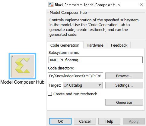
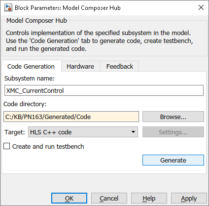
The first step of any Model Composer design is to add a Model Composer Hub which serves to configure the compilation of the design and the IP core generation. From this block, the following should be configured:
- The Subsystem name specifies the name of the top-level subsystem that will be used to generated the IP
- The Code directory defines where the IP sources will be generated
- The Target should be HLS C++ code. The reason is that Model Composer uses the HLS PIPELINE directive which cause problems in a control application such as our. Unfortunately, we have to go through Vitis HLS C++ to disable this directive. This issue is further explained in a section below.
- The Project device should be xc7z030fbg676-3
- The FPGA clock frequency should be 250 MHz
- The Throughput factor should be 1
Defining the IP input and output ports
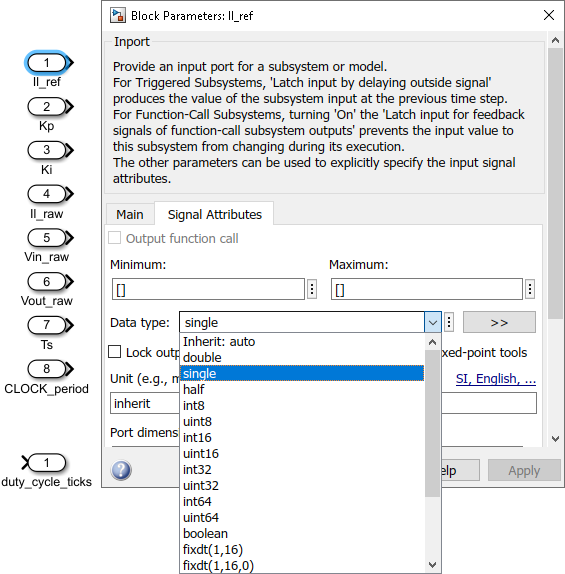
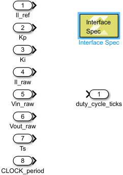
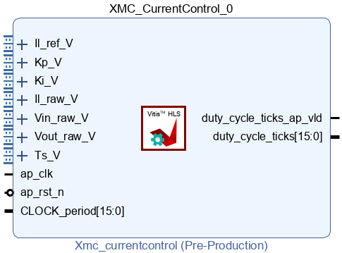
The user can then create a subsystem. In this example, the subsystem is called XMC_PI_floating (for Xilinx Model Composer PI using floating-point arithmetic). We’ll begin by specifying all the input and outputs of the IP. As shown in the screenshot below, the port data types are specified directly in the signal attributes of the Inports and Outports. We’ll use the following:
- The parameters coming from the CPU (
Il_ref,KpandKi) are set to single. - The inputs
Il_raw,Vin_rawandVout_rawwill be directly connected to the ADC interfaces and therefore must be set as int16. - The input
Tsis a uint32 value holding the sampling time in nanoseconds. - The input
CLOCK_periodis a uint16 value representing the PWM period in ticks. - The output
duty_cycle_ticksis a uint16 value that will be connected to the PWM IP.
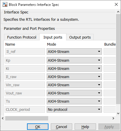
We then add an Interface Spec block that specifies the IP core interface protocols. We use the following configuration:
- Function Protocol
- We set the Function Protocol Mode to No block-level I/O protocol. We’ll use port-level protocol instead to tell the IP when it has to process data.
- Input ports
- After the user CPU code start, the
CLOCK_periodinput is constant. Thus, its mode is set to No protocol. - All the other inputs use the AXI4-Stream protocol.
- After the user CPU code start, the
- Output ports
- The
duty_cycle_ticksoutput uses the Valid Port mode. As shown on the very last image of this page, it will generate an additionnal “valid” portduty_cycle_ticks_ap_vldindicating when theduty_cycle_tickscan be read.
- The
Implementing the algorithm
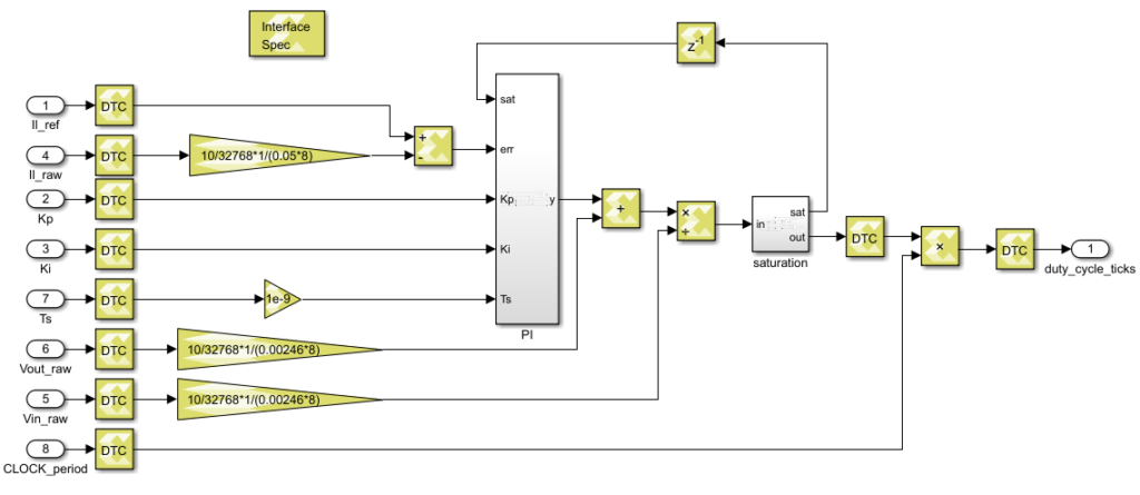
Below is shown the XMC_PI_floating subsystem. It shows that a Model Composer design is very similar to a standard Simulink design.
Here are some comments regarding this design:
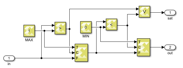
- All the inputs except CLOCK_period are converted to the single data type using data type conversion (DTC) blocks. When developing a new design, we recommend using single-precision floating-point as much as possible, as this makes the design much less prone to errors. Once the design has been validated, its latency and resource usage can be further optimized by converting parts of it to fixed-point arithmetic.
- The ADC values provided by the starter template (
Il_raw,Vin_rawandVout_raw) are the raw results from the ADC chips. They are multiplied by a gain inside the IP to obtain physical values. An example of gain computation is available on the ADC block help page. To simplify the model, the ADC gains are defined as constants, and offsets are simply ignored. The user could choose to use tunable parameters coming from the CPU so that the ADC can be tuned in real-time. - The Ts input provided a value in nanoseconds. It is multiplied by 1e-9 to obtain a value in seconds.
- A DTC block is used to transform the single output of the saturation block into a fixed point value. Indeed, the output of the saturation block is a duty cycle ranging from 0.0 to 1.0. Such a narrow range is particularly well-suited for a fixed-point algorithm, as we know beforehand that only a single bit is required for the integer part. We arbitrarily choose a fractional length of 15 bits so we obtain a fix16_15 value. This value is then multiplied by the CLOCK_period, which is a uint16 value, resulting in a fix32_15 (32-bit, 17-bit integer part, and 15-bit fractional part). Since the output is a number of ticks, it must be an integer value, and the fractional part is removed by simply transforming the result into a uint16 using a DTC block.
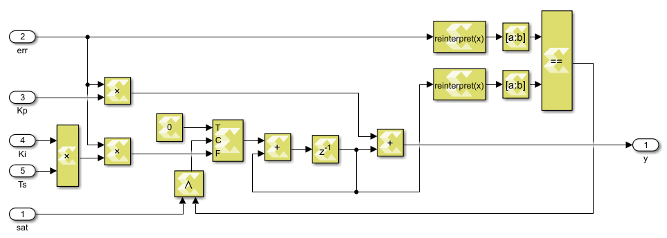
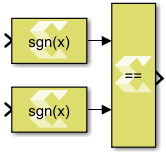
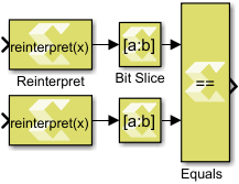
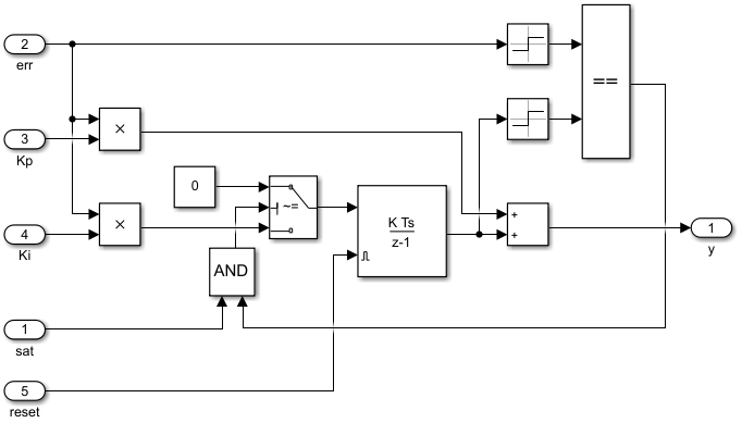
- In the PI subsystem, a comparison is done between the sign of the error and the sign of the integrator. Below are shown two possible implementations for such a comparison. The left option use the signum block which outputs a single value. On the right is shown a much more FPGA-optimized implementation in which the sign bits are directly compared. The reinterpret blocks are required because the bit slice does not support floating point inputs.
Verifying the design in simulation
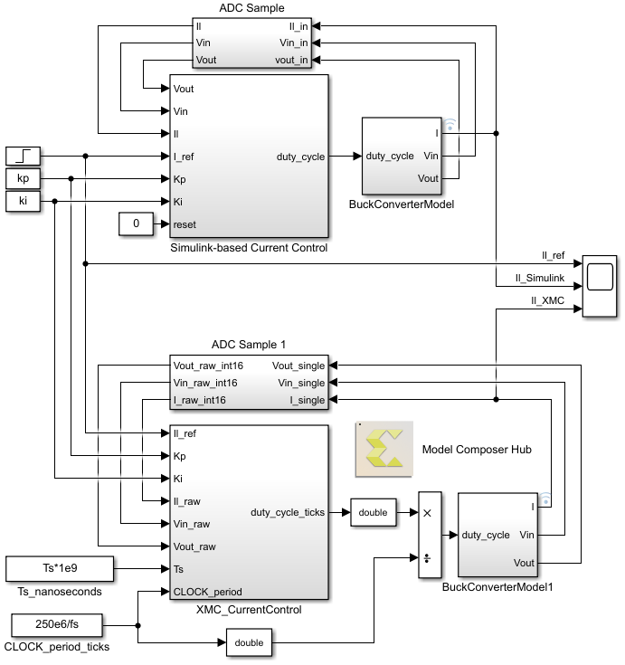
A Model Composer model can be verified using standard Simulink simulation. It allows to easily generate stimulus inputs and observe the results. Below is shown the test bench that is used to validate the proper functioning of the Model Composer implementation of the FPGA current control. It compares the result of the already-tested Simulink implementation of the basic PI-control technical note with the Model Composer design.
The screenshot below shows the buck converter model used to validate the current control algorithm. It also simulates the PWM generation. The outputs of this model are continuous values in volts or amperes. The ADC sample subsystem models the ADC chips behavior by transforming the continuous physical values into sampled int16 values.
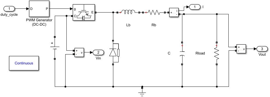
Simscape Electrical Specialized Power Systems library
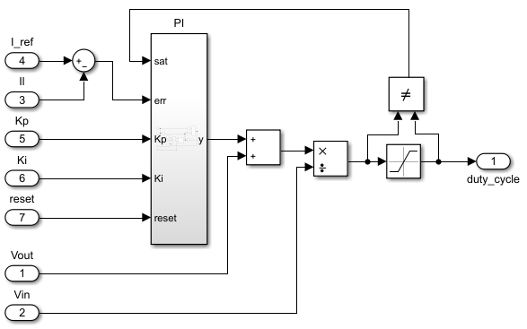
The Simulink-based current control algorithm that serves as the reference implementation is shown below.
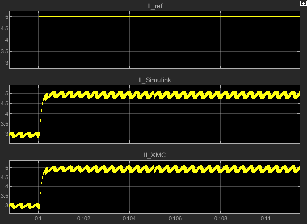
The reference current input is stepped from 3 A to 5 A. It can be observed that both implementations are behaving very similarly.
Generating an IP core using Model Composer
As mentioned earlier, Model Composer is an automated generation code tool based on Vivado HLS C++. Unfortunately, Model Composer uses the #pragma HLS PIPELINE directive by default which causes issues in our use case.
Why is the HLS PIPELINE pragma an issue?
The PIPELINE primitive reduces the initiation interval (II). In other words, it increases the maximal throughput of the IP by reducing the number of clock cycles between each input. The side effect is that the data is “stuck” in the IP until new data is fed to the input. For instance, if the IP latency is 10, then the result for the 1st data will be available only after the 10th data has been loaded into the IP. This is suitable for applications such as video processing where the data stream is constant and throughput optimization is most important. However, in a closed-loop control system such as ours, this behavior is not adequate, so we need to remove the HLS PIPELINE directive.
For more information on the PIPELINE directive, please refer to the Xilinx HLS pragmas documentation.
IP core generation step-by-step procedure
- Open the Model Composer Hub
- make sure the target is HLS C++ code
- select a code directory, for instance
C:/KnowledgeBase/XMC/PiCtrl/Code - click Generate
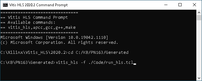
- Launch the Vitis HLS Command Prompt program
- Change the directory to the parent folder of the code directory specified above
cd C:/KB/PN163/Generated- Launch the run_hls.tcl script, which creates a Vitis HLS project
vitis_hls -f ./Code/run_hls.tcl- Open the freshly created project with Vitis HLS by running the command below. (Alternatively, the project can be manually opened from Vitis HLS.)
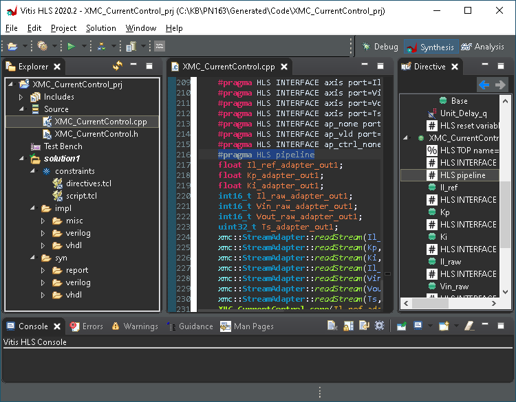
vitis_hls -p ./Code/XMC_CurrentControl_prj- To remove the HLS pipeline directive:
- Open the source file
XMC_CurrentControl.cpp. - Open the tab Directive on the right.
- Find the HLS pipeline directive, right click and hit “Remove directive”. Alternatively, the line e
#pragma HLS pipelinecan be manually removed from the C++ code. - Save the project (Ctrl+S).
- Open the source file
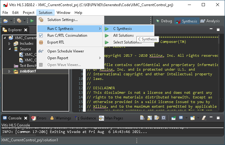
- Launch the C Synthesis by going to Solution -> Run C Synthesis -> Active Solution
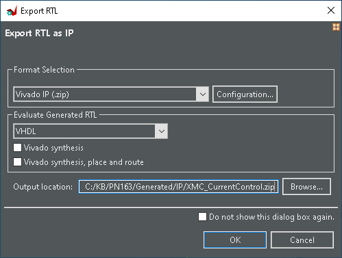
- Once the synthesis is done, export the RTL using the Vivado IP format
- Click Solution -> Export RTL,
- Select the Vivado IP (.zip) format,
- The generated RTL can be VHDL or Verilog, it does not matter.
- Choose an output location, for instance
C:/KB/PN163/Generated/IP
- Click OK.
Performance and resource estimates
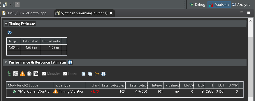
The FPGA of imperix controllers (part: xc7z030fbg676-3) possesses 78600 LUT, 157200 FF and 400 DSP, from which around ~30% is used by the imperix firmware IP. By clicking on Solution -> Open Report -> Synthesis, the user has access to the synthesis summary report which estimates the IP latency and resource usage. Make sure that the Pipelined option is set to no.
Our IP shows the following estimation: 3460 LUT (4.4% of total), 2988 FF (1.9%), and 9 DSP (2.3%).
Adding the IP core to a Vivado project
To interconnect the generated IP with other IPs, it needs to be added to a Vivado project. To do, in Vivado:
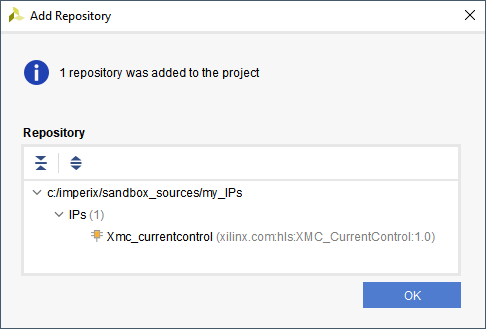
- Unzip the file generated by Vitis HLS (XMC_CurrentControl.zip),
- Go to the IP Catalog,
- Right-click and select Add Repository…
- Select the folder containing your unzipped IP (e.g.
C:\imperix\sandbox_sources\my_IPs). This folder can cotain multiple IPs.
- And finally the IP can be added to a block design like any other Xilinx IP.
To see this IP in action please refer to the FPGA current control using high-level synthesis page.


