Table of Contents
This technical note shows how the implementation of an FPGA-based hysteresis controller can be conducted, starting from the modeling stage, following with automated VHDL code generation with HDL Coder, and finishing with its validation in simulation. As an application example, this note uses the hysteresis current control already shown in TN120.
HDL Coder is a MATLAB tool that generates HDL code from Matlab or Simulink models, which can then be integrated into an FPGA. This approach can greatly accelerate rapid prototyping as the design is performed from a higher level of abstraction. The second benefit is the possibility to simulate the FPGA logic in a control loop, directly from within Simulink.
Software resources
FPGA logic implementation
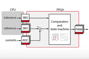
Below is the hysteresis current controller (also called direct current control [DCC]) logic implementation is taken from TN120.
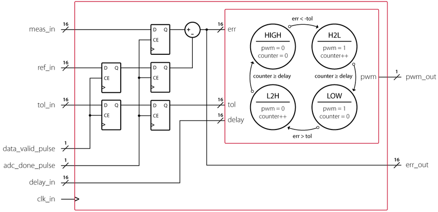
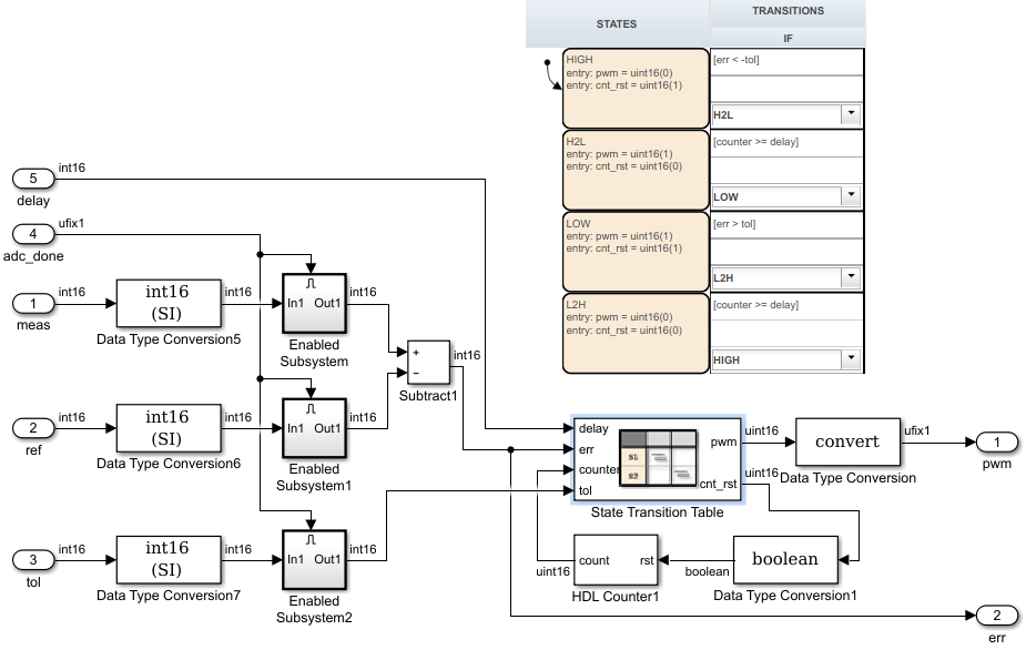
An equivalent logic can be transcribed in Simulink using HDL Coder-compatible blocks, as shown in the next figure. The Data Type Conversion blocks force the input signals to be interpreted as signed integers, the Enabled Subsystems infer the flip-flop registers, and the Stateflow’s State Transition Table block is used to easily implement the state machine.
Validation of the FPGA-based hysteresis controller by simulation
The validation of the FPGA-based hysteresis controller is done in two phases. First, the design is placed in a testbench model and stimulated with various test signals. The second phase is the integration of the design in the control model to simulate its behavior in a closed control loop.
Testbench
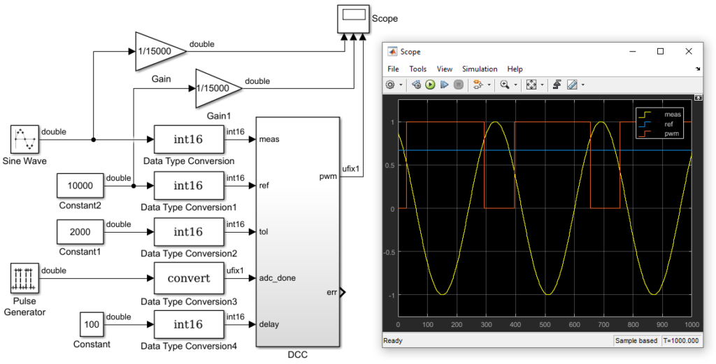
The tests must be as comprehensive as possible to see if the design operates as expected in all conditions. The following figure illustrates one of the validation steps, where the state machine transitions are tested by applying a sinusoidal signal to meas and a fixed value to the other inputs. The results are visually inspected using a scope that shows that the PWM signal has the correct state and the transition occurs when the difference between meas and ref is equal to tol.
Control loop simulation
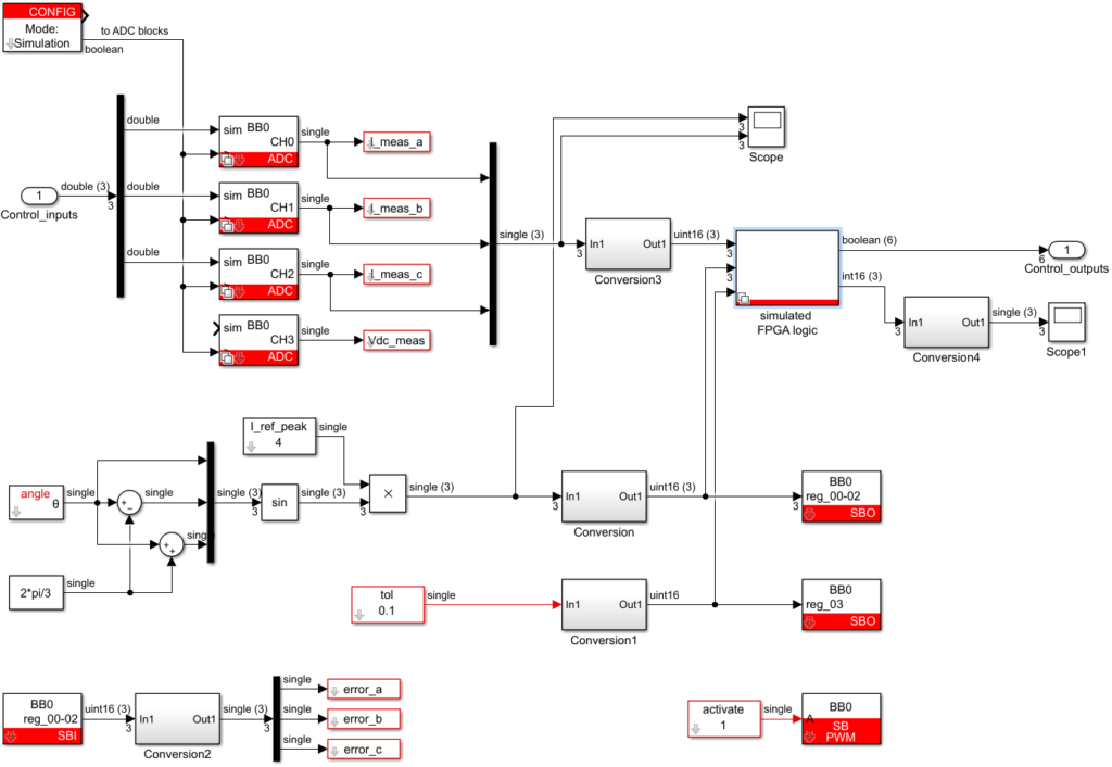
The second phase is the integration of this design within the control model already used in TN120. The objective is to simulate its behavior in a closed control loop. The simulated FPGA logic block takes as input the ADC values, scaled to match the actual 16-bit ADC output provided by the imperix firmware IP, as well as the values applied to the SBO blocks. The PWM output is conveyed to the plant model.
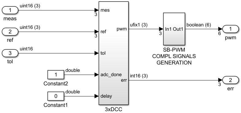
The content of the simulated FPGA logic block is shown in the next figure. It contains three instances of the DCC subsystem and a complementary PWM signal generation system. Due to the time scale of a control simulation, it is impractical to simulate the behavior of adc_done and the delay. To ignore them, they have been set to 1 and 0, respectively.
The sampling frequency (CLOCK_0) has been set to 400 kHz but the postscaler has been kept to 0 to simulate the “fast” FPGA logic. To emulate the “slow” logic reference generation (40kHz), the angle block has been configured to have a sample time of ten times the sampling frequency. Further details regarding this configuration can be found in TN120.
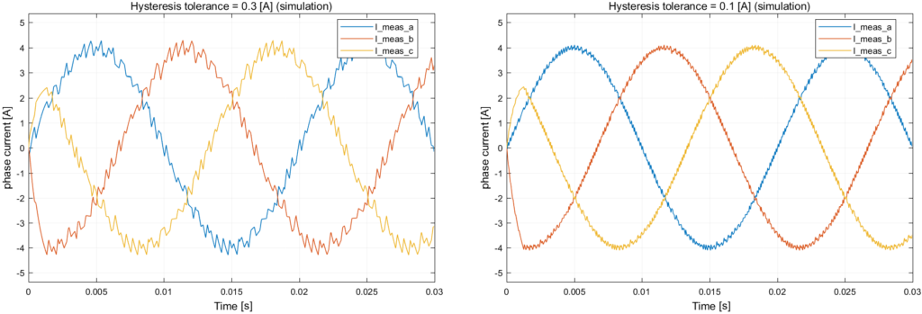
The following graphs show the simulation results for a current reference of 4 A and a hysteresis tolerance of ±0.3 A and ±0.1 A, which are very close to the experimental measurements of TN120.
Integration of the HDL design in the FPGA firmware
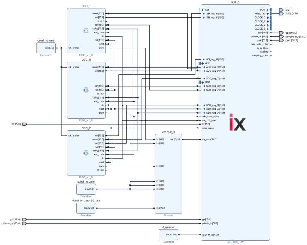
Once the implementation has been validated in simulation, the VHDL sources can be generated and integrated into the sandbox environment, as shown in the next figure. Step-by-step instructions, as well as general design recommendations regarding the implementation of custom FPGA firmware, can be found in PN116.


