FPGA-based SPI communication IP for ADC

This technical note shows how an SPI communication link can be established between an FPGA and an external Analog-to-Digital Converter (ADC). The development setup will consist of an imperix B-Board PRO evaluation kit and an LTC2314 demonstration circuit. The LTC2314 ADC driver will be developed using VHDL integrated into the user-programmable area (the sandbox) of the FPGA thanks to the FPGA customization feature of the imperix controllers. Three of the 36 user-configurable 3.3V I/Os of the B-Board will be used for the SPI communication with the ADC.

This note provides a VHDL implementation of the FPGA ADC driver. However, automated HDL code generation tools such as MATLAB HDL Coder or Xilinx System Generator can be used to create FPGA peripherals as shown on the custom FPGA PWM page.

Information on how to set up the toolchain for the FPGA programming is available on the Vivado Design Suite installation page.

Quick-start information on how to use the sandbox is provided on the getting started with FPGA page.

Software resources

The FPGA ADC driver resources can be downloaded by clicking on the button below. It contains the VHDL driver LT2314_driver.vhd, its associated testbench LT2314_tb.vhd, as well as the C++ drivers implemented using the C++ SDK.

FPGA ADC implementation

This example implements a full-custom FPGA ADC SPI driver for the LTC2314-14 serial sampling ADC with the following settings:

  • It uses the LTC2314 SCK continuous mode (see next figure)
  • The SCK frequency is configurable using a postscaler (postscaler_in)
  • The conversion is started upon the assertion of sampling_pulse
LTC2314-14 Serial Interface Timing Diagram in SCK Continuous Mode
LTC2314-14 Serial Interface Timing Diagram in SCK Continuous Mode (source LTC2314 datasheet)
library IEEE;
use IEEE.STD_LOGIC_1164.ALL;
use IEEE.NUMERIC_STD.ALL;
 
entity LT2314_driver is
port(
    -- CLOCKS:
    clk_250: in std_logic; -- 250 MHz clock
    sampling_pulse: in std_logic; -- sampling strobe
 
    -- CONFIGURATION:
    -- spi_sck = clk_250 / (postscaler_in*2)
    postscaler_in: in std_logic_vector(15 downto 0);
 
    -- OUTPUT DATA:
    data_out: out std_logic_vector(15 downto 0) := (others => '0');
 
    -- SPI SIGNALS:
    spi_sck: out std_logic; -- communication clock
    spi_cs_n: out std_logic; -- chip select strobe / sampling trigger
    spi_din: in std_logic -- serial data in
);
end LT2314_driver;
 
architecture impl of LT2314_driver is
 
    TYPE states is (ACQ,CONV);
 
    SIGNAL state : states := ACQ; -- FSM state register
 
    -- Signal used as SPI communication clock
    -- spi_sck = postscaled_clk = clk_250 / (postscaler_in*2)
    SIGNAL postscaled_clk : std_logic := '0';
 
    -- Indicates a rising edge on postscaled_clk
    SIGNAL postscaled_clk_rising_pulse : std_logic := '0';
 
    -- Asserted when sampling_pulse = '1'
    -- Cleared when postscaled_clk_rising_pulse = '1'
    SIGNAL pulse_detected : std_logic := '0';
begin
 
    spi_sck <= postscaled_clk;
    spi_cs_n <= '1' when state=ACQ else '0';
 
    -- Generate postscaled_clk and postscaled_clk_rising_pulse
    POSTSCALER: process(clk_250)
        variable postscaler_cnt: unsigned(15 downto 0):=(others=>'0');
    begin
        if rising_edge(clk_250) then
            postscaled_clk_rising_pulse <= '0';
 
            -- Toggle postscaled_clk
            -- Assert postscaled_clk_rising_pulse if rising edge
            if postscaler_cnt+1 >= unsigned(postscaler_in) then
                if postscaled_clk = '0' then
                    postscaled_clk_rising_pulse <= '1';
                end if;
                postscaler_cnt := (others => '0');
                postscaled_clk <= not postscaled_clk;
            else
                postscaler_cnt := postscaler_cnt + 1;
            end if;
        end if;
    end process POSTSCALER;
 
    -- Generate pulse_detected
    SAMPLING: process(clk_250)
    begin
        if rising_edge(clk_250) then
            if sampling_pulse = '1' then
                pulse_detected <= '1';
            elsif postscaled_clk_rising_pulse = '1' then
                pulse_detected <= '0';
            end if;
        end if;
    end process SAMPLING;
 
    -- Finite State Machine
    -- Run at SPI clock speed (using postscaled_clk_rising_pulse=
    FSM : process(clk_250)
        variable bit_cnt : unsigned(4 downto 0) := (others=>'0'); -- bit counter
    begin
        if rising_edge(clk_250) and postscaled_clk_rising_pulse = '1' then
            case state is
 
                when ACQ =>
                    bit_cnt := (others => '0');
                    if pulse_detected = '1' then
                        state <= CONV;
                    end if;
 
                when CONV =>
                    bit_cnt := bit_cnt + 1;
                    if bit_cnt >= 16 then
                        state <= ACQ;
                    end if;
 
                when others => null;
            end case;
        end if;
    end process FSM;
 
    -- Sample spi_din on spi_sck rising edge during ACQUISITION phase
    SHIFT_REG: process (clk_250)
        variable data_reg: std_logic_vector(15 downto 0):=(others=>'0');
    begin
        if rising_edge(clk_250) then
            if state = CONV and postscaled_clk_rising_pulse = '1' then
                data_reg := data_reg(14 downto 0) & spi_din;
            elsif state = ACQ then
                data_out <= "0" & data_reg(15 downto 1); -- re-align data
            end if;
        end if;
    end process SHIFT_REG;
end impl;Code language: VHDL (vhdl)

FPGA ADC testbench

A VHDL testbench modeling the LTC2314 behavior has been written in order to validate the FPGA ADC driver behavior.

library IEEE;
use IEEE.STD_LOGIC_1164.ALL;
use IEEE.NUMERIC_STD.ALL;
 
entity LT2314_tb is end;
 
architecture bench of LT2314_tb is
     
    -- number of blank bits provided by the ADC
    constant NBLANKBITS : positive := 1;
     
    -- SCK = CLK_250_MHZ / (POSTSCALER*2) = 62.5 MHz
    constant SCK_POSTSCALER : std_logic_vector := "0000000000000010";
     
    -- main clock period
    constant CLK_PERIOD : time := 4.0 ns; -- 250 MHz
     
    -- simulated data sample produced by the ADC
    signal rawdata : unsigned(13 downto 0) := (others=>'0');
     
    -- clock signals
    signal clk_250, sampling_pulse : std_logic := '0';
     
    -- SPI signals
    signal SPI_DIN, SPI_nCS, SPI_CLK : std_logic := '0';
     
begin
         
    primary_clock: clk_250 <= not clk_250 after CLK_PERIOD / 2;
         
    --------------------------------------------------------------------------------
    -- DEVICE UNDER TEST
    --------------------------------------------------------------------------------
         
    DUT: entity work.LT2314_driver
    port map(
        clk_250 => clk_250,
        sampling_pulse => sampling_pulse,
        postscaler_in => SCK_POSTSCALER,
        spi_sck => SPI_CLK,
        spi_cs_n => SPI_nCS,
        spi_din => SPI_DIN,
        data_out => open);
         
    --------------------------------------------------------------------------------
    -- ANALOG-TO-DIGITAL CONVERTER MODEL
    --------------------------------------------------------------------------------
         
    DATA_SAMPLE: process
    begin
        wait for CLK_PERIOD*100;
             
        rawdata <= to_unsigned(12345,14);
        sampling_pulse <= '1';
        wait for CLK_PERIOD;
        sampling_pulse <= '0';
             
        wait for CLK_PERIOD*100;
             
        rawdata <= to_unsigned(5782,14);
        sampling_pulse <= '1';
        wait for CLK_PERIOD;
        sampling_pulse <= '0';
             
        wait for CLK_PERIOD*100;
             
        rawdata <= to_unsigned(777,14);
        sampling_pulse <= '1';
        wait for CLK_PERIOD;
        sampling_pulse <= '0';
             
    end process DATA_SAMPLE;
         
    SPI_TARGET: process(SPI_nCS,SPI_CLK,SPI_DIN)
    variable counter : integer := 0;
    begin
        if SPI_nCS='1' then
            SPI_DIN <= 'Z';
            counter := 13 + NBLANKBITS;
        elsif SPI_nCS='0' and falling_edge(SPI_CLK) then
            if (counter > 13 or counter < 0) then
                SPI_DIN <= '0';
            else
                SPI_DIN <= std_logic(rawdata(counter));
            end if;
            counter := counter - 1;
        end if;
    end process SPI_TARGET;
         
end architecture bench;Code language: VHDL (vhdl)
SPI communication testbench results

Deployment on the B-Board PRO FPGA

To learn how to add a VHDL module into B-Board FPGA firmware using Xilinx Vivado, please read the getting started with FPGA page. The ADC SPI driver has interfaced as follow:
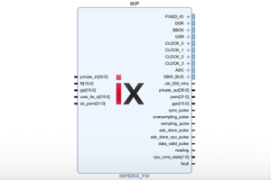
  • spi_sck is connected to the physical pin USR[0]
  • spi_cs_n is connected to the physical pin USR[1]
  • spi_din is connected to the physical pin USR[2]
  • postscaler_in is connected to SBO_reg_00 (configuration register)
  • data_out is connected to SBI_reg_00 (real-time register)

Furthermore, the signals spi_sck, spi_cs_n, spi_din, data_out and sampling_pulse are also connected to an Integrated Logic Analyzer (ILA), allowing them to be observed during run-time.

Interfacing between the SPI driver and imperix IP
Interfacing of the ADC driver in the B-Board FPGA

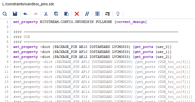
Using the imperix 3.3V USR pins

The SPI signals (SCK, nCS, and MISO) of the ADC driver are connected to 3 of the 36 user-configurable 3.3V I/Os of the B-Board (usr_0, usr_1, and usr_2). The physical pin constraint file sandbox_pins.xdc file must be edited by the user to match the external port names.

Experimental results

The following hardware was used:

  • B-Board evaluation kit
  • LTC2314 demonstration circuit
  • Xilinx JTAG Platform Cable USB II
  • DSLogic Plus logic analyzer
Experimental setup of the SPI communication

The following C++ code has been used to test the LT2314 driver.

define ADC_GAIN (4.096/8192.0)
 
int adc_raw;
float Vmeas;
 
tUserSafe UserInit(void)
{
  Clock_SetFrequency(CLOCK_0, 20e3);
  ConfigureMainInterrupt(UserInterrupt, CLOCK_0, 0.5);
 
  Sbi_ConfigureAsRealTime(0); // SBI_reg_00 contains the ADC value (LT2314_driver data_out)
  Sbo_WriteDirectly(0, 2);    // SBO_reg_00 is the clk postscaler (LT2314_driver postscaler_in)
                              // postscaler = 2 -> SCK = 62.5 MHz
  return SAFE;
}
 
tUserSafe UserInterrupt(void)
{
  adc_raw = Sbi_Read(0); // read SBI_reg_00
  Vmeas = adc_raw * ADC_GAIN; // convert to Volts
 
  return SAFE;
}Code language: C++ (cpp)

The external SPI signals can be observed using a physical logic analyzer such as the DSLogic Plus:

Experimental results from logic analyzer of the SPI communication

Secondly, the Xilinx Integrated Logic Analyzer (ILA) allows to observe internal signals too:

Experimental results from Xilinx Integrated Logic Analyzer of the SPI communication

Finally, the end result can be plotted in the Cockpit monitoring software, attesting that the SPI module works correctly.